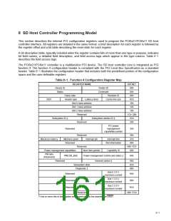
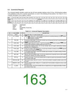
8.4 Status Register
The status register provides device information to the host system. All bit functions adhere to the definitions in the
PCI Local Bus Specification, as seen in the following bit descriptions. Bits in this register may be read normally. A
bit in the status register is reset when a 1 is written to that bit location; a 0 written to a bit location has no effect. See
Table 8−3 for a complete description of the register contents.
Bit
15
14
13
12
11
10
9
8
7
6
5
4
3
2
1
0
Name
Type
Default
Status
RCU RCU RCU RCU RCU
R
0
R
1
RCU
0
R
0
R
0
R
0
R
1
RU
0
R
0
R
0
R
0
0
0
0
0
0
Register:
Offset:
Type:
Status
06h
Read/Clear/Update, Read-only
0210h
Default:
Table 8−3. Status Register Description
BIT
15
FIELD NAME
PAR_ERR
TYPE
RCU
RCU
DESCRIPTION
Detected parity error. Bit 15 is set to 1 when either an address parity or data parity error is detected.
14
SYS_ERR
Signaled system error. Bit 14 is set to 1 when SERR is enabled and the SD host controller has signaled
a system error to the host.
13
12
MABORT
TABORT_REC
TABORT_SIG
PCI_SPEED
DATAPAR
RCU
RCU
RCU
R
Received master abort. Bit 13 is set to 1 when a cycle initiated by the SD host controller on the PCI
bus has been terminated by a master abort.
Received target abort. Bit 12 is set to 1 when a cycle initiated by the SD host controller on the PCI bus
was terminated by a target abort.
11
Signaled target abort. Bit 11 is set to 1 by the SD host controller when it terminates a transaction on
the PCI bus with a target abort.
10−9
8
DEVSEL timing. Bits 10 and 9 encode the timing of DEVSEL and are hardwired to 01b, indicating that
the SD host controller asserts this signal at a medium speed on nonconfiguration cycle accesses.
RCU
Data parity error detected. Bit 8 is set to 1 when the following conditions have been met:
a. PERR was asserted by any PCI device including the SD host controller.
b. The SD host controller was the bus master during the data parity error.
c. Bit 6 (PERR_EN) in the command register at offset 04h in the PCI configuration space
(see Section 8.3) is set to 1.
7
6
5
4
3
FBB_CAP
UDF
R
R
Fast back-to-back capable. The SD host controller cannot accept fast back-to-back transactions;
therefore, bit 7 is hardwired to 0.
User-definable features (UDF) supported. The SD host controller does not support the UDF; therefore,
bit 6 is hardwired to 0.
66MHZ
R
66-MHz capable. The SD host controller operates at a maximum PCLK frequency of 33 MHz;
therefore, bit 5 is hardwired to 0.
CAPLIST
INT_STATUS
R
Capabilities list. Bit 4 returns 1 when read, indicating that the SD host controller supports additional
PCI capabilities.
RU
Interrupt status. This bit reflects the interrupt status of the function. Only when bit 10 (INT_DISABLE)
in the command register (see Section 8.3) is a 0 and this bit is 1, is the function’s INTx signal asserted.
Setting the INT_DISABLE bit to 1 has no effect on the state of this bit. This bit is set only when a valid
interrupt condition exists. This bit is not set when an interrupt condition exists and signaling of that event
is not enabled.
2−0
RSVD
R
Reserved. Bits 3−0 return 0s when read.
8−4

 TI [ TEXAS INSTRUMENTS ]