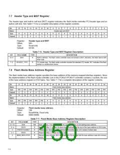
7.7 Header Type and BIST Register
The header type and built-in self-test (BIST) register indicates the flash media controller PCI header type and no
built-in self-test. See Table 7−6 for a complete description of the register contents.
Bit
15
14
13
12
11
10
9
8
7
6
5
4
3
2
1
0
Name
Type
Default
Header type and BIST
R
0
R
0
R
0
R
0
R
0
R
0
R
0
R
0
R
1
R
0
R
0
R
0
R
0
R
0
R
0
R
0
Register:
Offset:
Type:
Header type and BIST
0Eh
Read-only
0010h
Default:
Table 7−6. Header Type and BIST Register Description
BIT
FIELD NAME
TYPE
DESCRIPTION
15−8
BIST
R
Built-in self-test. The flash media controller does not include a BIST; therefore, this field returns 00h
when read.
7−0
HEADER_TYPE
R
PCI header type. The flash media controller includes the standard PCI header. Bit 7 indicates if the flash
media is a multifunction device.
7.8 Flash Media Base Address Register
The flash media base address register specifies the base address of the memory-mapped interface registers. Since
the implementation of the flash media controller core in the PCI6x21/PCI6x11 controller contains 2 sockets, the size
of the base address register is 8192 bytes. See Table 7−7 for a complete description of the register contents.
Bit
31
30
29
28
27
26
25
24
23
22
21
20
19
18
17
16
Name
Type
Default
Flash media base address
RW
0
RW
0
RW
0
RW
0
RW
0
RW
0
RW
0
RW
0
RW
0
RW
0
RW
0
RW
0
RW
0
RW
0
RW
0
RW
0
Bit
15
14
13
12
11
10
9
8
7
6
5
4
3
2
1
0
Name
Type
Default
Flash media base address
RW
0
RW
0
RW
0
RW
0
RW
0
R
0
R
0
R
0
R
0
R
0
R
0
R
0
R
0
R
0
R
0
R
0
Register:
Offset:
Type:
Flash media base address
10h
Read/Write, Read-only
0000 0000h
Default:
Table 7−7. Flash Media Base Address Register Description
BIT
31−12
11−4
3
FIELD NAME
BAR
TYPE
RW
R
DESCRIPTION
Base address. This field specifies the upper bits of the 32-bit starting base address.
RSVD
Reserved. Bits 11−4 return 0s when read to indicate that the size of the base address is 8192 bytes.
Prefetchable. Since this base address is not prefetchable, bit 3 returns 0 when read.
Reserved. Bits 2−1 return 0s when read.
PREFETCHABLE
RSVD
R
2−1
0
R
MEM_INDICATOR
R
Memory space indicator. Bit 0 is hardwired to 0 to indicate that the base address maps into memory
space.
7−6

 TI [ TEXAS INSTRUMENTS ]