ONET1131EC
www.ti.com.cn
ZHCSFG0 –SEPTEMBER 2016
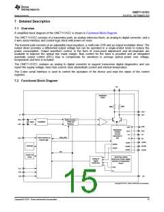
7 Detailed Description
7.1 Overview
A simplified block diagram of the ONET1131EC is shown in Functional Block Diagram.
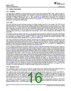
The ONET1131EC consists of a transmitter path, an analog reference block, an analog to digital converter, and a
2-wire serial interface and control logic block with power-on reset.
The transmit path consists of an adjustable input equalizer, a multi-rate CDR and an output modulator driver. The
output driver provides a differential output voltage but can be operated in a single-ended mode to reduce the
power consumption. Output waveform control, in the form of cross-point adjustment and de-emphasis are
available to improve the optical eye mask margin. Bias current for the laser is provided and an integrated
automatic power control (APC) loop to compensate for variations in average optical power over voltage,
temperature and time is included.
The ONET1131EC contains an analog to digital converter to support transceiver digital diagnostics and can
report the supply voltage, laser bias current, laser photodiode current and internal temperature.
The 2-wire serial interface is used to control the operation of the device and read the status of the control
registers.
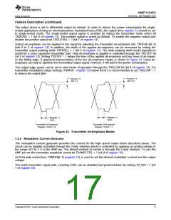
7.2 Functional Block Diagram
ë//
aodulꢀtor
5river
60ꢀ
60ꢀ
hÜÇ+
hÜÇ-
[C
5Lb+
5Lb-
Referenceless
CDR and
Retimer
Equalizer
100ꢀ
!at
!at
aodulꢀtion
ꢀnd .iꢀs
/urrent
Denerꢀtor &
!ꢁ/
.L!{
C[Ç
.L!{
C[Ç
t5
/5w_/Çw[
2-íire Lnterfꢀce &
/ontrol [ogic
ë55
t5
/hat
ahb.
/hat
ahb.
ahbt
99ꢁwha
ahb.
ahbt
ahbt
[h[
ꢁoꢂer-hn
weset
.ꢀnd-Dꢀp, !nꢀlog
!nꢀlog to
5igitꢀl
/onversion
weferences, ꢁoꢂer {upply
aonitor & Çemperꢀture
{ensor
t{a
Ç{
{/Y
{5!
[h[
DIS
Copyright © 2016, Texas Instruments Incorporated
Copyright © 2016, Texas Instruments Incorporated
15

 TI [ TEXAS INSTRUMENTS ]