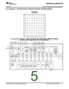
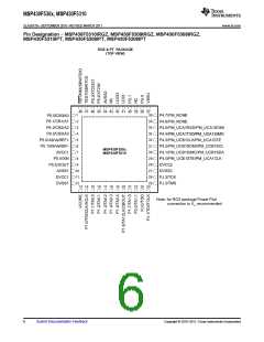
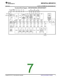
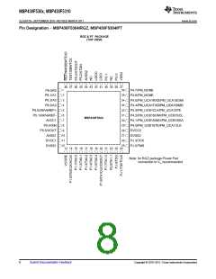
MSP430F530x, MSP430F5310
www.ti.com
SLAS677B –SEPTEMBER 2010–REVISED MARCH 2011
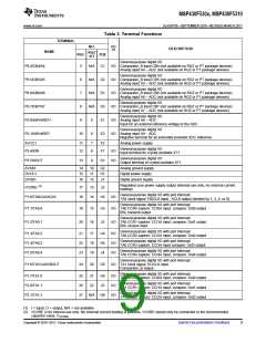
Table 3. Terminal Functions
TERMINAL
NO.
I/O
DESCRIPTION
(1)
NAME
RGZ
/PT
RGC
ZQE
General-purpose digital I/O
P6.4/CB4/A4
P6.5/CB5/A5
P6.6/CB6/A6
P6.7/CB7/A7
5
N/A
N/A
N/A
N/A
5
C1
D2
D1
D3
E1
E2
I/O Comparator_B input CB4 (not available on RGZ or PT package devices)
Analog input A4 – ADC (not available on RGZ or PT package devices)
General-purpose digital I/O
I/O Comparator_B input CB5 (not available on RGZ or PT package devices)
Analog input A5 – ADC (not available on RGZ or PT package devices)
6
7
General-purpose digital I/O
I/O Comparator_B input CB6 (not available on RGZ or PT package devices)
Analog input A6 – ADC (not available on RGZ or PT package devices)
General-purpose digital I/O
I/O Comparator_B input CB7 (not available on RGZ or PT package devices)
Analog input A7 – ADC (not available on RGZ or PT package devices)
8
General-purpose digital I/O
I/O Analog input A8 – ADC
P5.0/A8/VeREF+
P5.1/A9/VeREF-
9
Input for an external reference voltage to the ADC
General-purpose digital I/O
I/O Analog input A9 – ADC
10
6
Negative terminal for an externally provided ADC reference
AVCC1
11
12
7
8
F2
F1
Analog power supply
General-purpose digital I/O
I/O
P5.4/XIN
Input terminal for crystal oscillator XT1
General-purpose digital I/O
I/O
P5.5/XOUT
13
9
G1
Output terminal of crystal oscillator XT1
AVSS1
DVCC1
DVSS1
14
15
16
10
11
12
G2
H1
J1
Analog ground supply
Digital power supply
Digital ground supply
Regulated core power supply output (internal use only, no external current
loading)
(2)
VCORE
17
18
13
14
J2
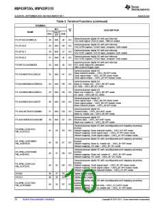
General-purpose digital I/O with port interrupt
TA0 clock signal TA0CLK input ; ACLK output (divided by 1, 2, 4, or 8)
P1.0/TA0CLK/ACLK
P1.1/TA0.0
H2
I/O
General-purpose digital I/O with port interrupt
I/O TA0 CCR0 capture: CCI0A input, compare: Out0 output
BSL transmit output
19
20
15
16
H3
J3
General-purpose digital I/O with port interrupt
I/O TA0 CCR1 capture: CCI1A input, compare: Out1 output
BSL receive input
P1.2/TA0.1
General-purpose digital I/O with port interrupt
TA0 CCR2 capture: CCI2A input, compare: Out2 output
P1.3/TA0.2
P1.4/TA0.3
P1.5/TA0.4
21
22
23
17
18
19
G4
H4
J4
I/O
General-purpose digital I/O with port interrupt
TA0 CCR3 capture: CCI3A input compare: Out3 output
I/O
General-purpose digital I/O with port interrupt
TA0 CCR4 capture: CCI4A input, compare: Out4 output
I/O
General-purpose digital I/O with port interrupt
I/O TA1 clock signal TA1CLK input
Comparator_B output
P1.6/TA1CLK/CBOUT
24
20
G5
General-purpose digital I/O with port interrupt
TA1 CCR0 capture: CCI0A input, compare: Out0 output
P1.7/TA1.0
P2.0/TA1.1
P2.1/TA1.2
25
26
27
21
22
H5
J5
I/O
General-purpose digital I/O with port interrupt
TA1 CCR1 capture: CCI1A input, compare: Out1 output
I/O
General-purpose digital I/O with port interrupt
TA1 CCR2 capture: CCI2A input, compare: Out2 output
N/A
G6
I/O
(1) I = input, O = output, N/A = not available
(2) VCORE is for internal use only. No external current loading is possible. VCORE should only be connected to the recommended
capacitor value, CVCORE
.
Copyright © 2010–2011, Texas Instruments Incorporated
Submit Documentation Feedback
9

 TI [ TEXAS INSTRUMENTS ]