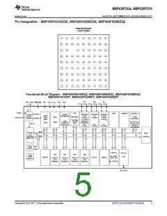
MSP430F530x, MSP430F5310
SLAS677B –SEPTEMBER 2010–REVISED MARCH 2011
www.ti.com
DESCRIPTION
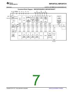
The Texas Instruments MSP430™ family of ultra-low-power microcontrollers consists of several devices featuring
different sets of peripherals targeted for various applications. The architecture, combined with five low-power
modes is optimized to achieve extended battery life in portable measurement applications. The device features a
powerful 16-bit RISC CPU, 16-bit registers, and constant generators that contribute to maximum code efficiency.
The digitally controlled oscillator (DCO) allows wake-up from low-power modes to active mode in less than 5 µs.
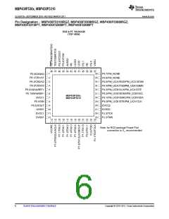
The MSP430F5310, MSP430F5309, and MSP430F5308 devices are microcontroller configurations with 3.3-V
LDO, four 16-bit timers, a high-performance 10-bit analog-to-digital converter (ADC), two universal serial
communication interfaces (USCI), hardware multiplier, DMA, real-time clock module with alarm capabilities and
31 or 47 I/O pins.
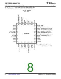
The MSP430F5304 device is a configuration 3.3-V LDO, four 16-bit timers, a high-performance 10-bit
analog-to-digital converter (ADC), two universal serial communication interfaces (USCI), hardware multiplier,
DMA, real-time clock module with alarm capabilities, and 31 I/O pins.
Typical applications for this device include analog and digital sensor systems, digital motor control, remote
controls, thermostats, digital timers, hand-held meters, etc.
Table 1. Family Members
USCI
PROGRAM
MEMORY
(KB)
SRAM
(KB)
ADC10_A
(CH)
Comp_B
(CH)
PACKAGE
TYPE
(1)
(2)
CHANNEL A: CHANNEL B:
UART/LIN/
DEVICE
Timer_A
5, 3, 3
Timer_B
I/O
SPI/I2C
IrDA/SPI
64 RGC,
80 ZQE
10 ext / 2 int
6 ext / 2 int
10 ext / 2 int
6 ext / 2 int
10 ext / 2 int
6 ext / 2 int
6 ext / 2 int
8
4
8
4
8
4
-
47
31
47
31
47
31
31
MSP430F5310
MSP430F5309
32
24
6
6
7
7
2
2
2
2
48 PT,
48 RGZ
64 RGC,
80 ZQE
5, 3, 3
48 PT,
48 RGZ,
64 RGC,
80 ZQE
MSP430F5308
MSP430F5304
16
8
6
6
5, 3, 3
5, 3, 3
7
7
2
1
2
1
48 PT,
48 RGZ,
48 PT,
48 RGZ
(1) Each number in the sequence represents an instantiation of Timer_A with its associated number of capture compare registers and PWM
output generators available. For example, a number sequence of 3, 5 would represent two instantiations of Timer_A, the first
instantiation having 3 and the second instantiation having 5 capture compare registers and PWM output generators, respectively.
(2) Each number in the sequence represents an instantiation of Timer_B with its associated number of capture compare registers and PWM
output generators available. For example, a number sequence of 3, 5 would represent two instantiations of Timer_B, the first
instantiation having 3 and the second instantiation having 5 capture compare registers and PWM output generators, respectively.
(1)
Table 2. Ordering Information
(2)
PACKAGED DEVICES
TA
PLASTIC 64-PIN VQFN
(RGC)
PLASTIC 80-BALL BGA
(ZQE)
PLASTIC 48-PIN VQFN
(RGZ)
PLASTIC 48-PIN LQFP
(PT)
MSP430F5310IRGC
MSP430F5309IRGC
MSP430F5308IRGC
MSP430F5310IZQE
MSP430F5309IZQE
MSP430F5308IZQE
MSP430F5310IRGZ
MSP430F5309IRGZ
MSP430F5308IRGZ
MSP430F5304IRGZ
MSP430F5310IPT
MSP430F5309IPT
MSP430F5308IPT
MSP430F5304IPT
–40°C to 85°C
(1) For the most current package and ordering information, see the Package Option Addendum at the end of this document, or see the TI
web site at www.ti.com.
(2) Package drawings, standard packing quantities, thermal data, symbolization, and PCB design guidelines are available at
www.ti.com/package.
2
Submit Documentation Feedback
Copyright © 2010–2011, Texas Instruments Incorporated

 TI [ TEXAS INSTRUMENTS ]