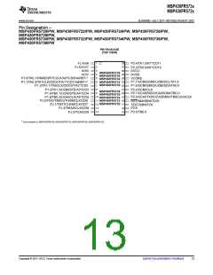
MSP430FR573x
MSP430FR572x
www.ti.com
SLAS639D –JULY 2011–REVISED AUGUST 2012
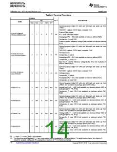
Table 4. Terminal Functions (continued)
TERMINAL
(1)
NO.
DA
I/O
DESCRIPTION
NAME
RHA RGE
PW
YFF
General-purpose digital I/O with port interrupt and wake up from
LPMx.5 (not available on package options PW, RGE)
P3.5/TB1.2/CDOUT
25
N/A
27
N/A
N/A
I/O
TB1 CCR2 capture: CCI2B input, compare: Out2 (not available on
devices without TB1)
Comparator_D output (not available on package options PW, RGE)
General-purpose digital I/O with port interrupt and wake up from
LPMx.5 (not available on package options PW, RGE)
TB2 CCR1 capture: CCI1B input, compare: Out1 (not available on
devices without TB2)
P3.6/TB2.1/TB1CLK
26
27
N/A
N/A
28
29
N/A
N/A
N/A
N/A
I/O
I/O
TB1 clock input (not available on devices without TB1 or package
options PW, RGE)
General-purpose digital I/O with port interrupt and wake up from
LPMx.5 (not available on package options PW, RGE)
P3.7/TB2.2
TB2 CCR2 capture: CCI2B input, compare: Out2 (not available on
devices without TB2 or package options PW, RGE)
General-purpose digital I/O with port interrupt and wake up from
LPMx.5
TB1 CCR1 capture: CCI1A input, compare: Out1 (not available on
devices without TB1)
P1.6/TB1.1/UCB0SIMO/
UCB0SDA/TA0.0
28
16
30
22
E2
I/O
Slave in, master out – eUSCI_B0 SPI mode
I2C data – eUSCI_B0 I2C mode
TA0 CCR0 capture: CCI0A input, compare: Out0
General-purpose digital I/O with port interrupt and wake up from
LPMx.5
TB1 CCR2 capture: CCI2A input, compare: Out2 (not available on
devices without TB1)
P1.7/TB1.2/UCB0SOMI/
UCB0SCL/TA1.0
29
17
31
23
E3
I/O
Slave out, master in – eUSCI_B0 SPI mode
I2C clock – eUSCI_B0 I2C mode
TA1 CCR0 capture: CCI0A input, compare: Out0
Regulated core power supply (internal use only, no external current loading)
Digital ground supply
(6)
VCORE
30
31
32
18
19
20
32
33
34
24
25
26
E1
D2
D1
DVSS
DVCC
Digital power supply
General-purpose digital I/O with port interrupt and wake up from LPMx.5 (not
available on package options PW, RGE)
P2.7
33
N/A
35
N/A
N/A
I/O
I/O
General-purpose digital I/O with port interrupt and wake up from
LPMx.5 (not available on package options RGE)
TA0 CCR0 capture: CCI0B input, compare: Out0 (not available on
package options RGE)
P2.3/TA0.0/UCA1STE/
A6/CD10
34
N/A
36
27
N/A
Slave transmit enable – eUSCI_A1 SPI mode (not available on
devices without eUSCI_A1)
Analog input A6 – ADC (not available on devices without ADC)
Comparator_D input CD10 (not available on package options RGE)
General-purpose digital I/O with port interrupt and wake up from
LPMx.5 (not available on package options RGE)
TA1 CCR0 capture: CCI0B input, compare: Out0 (not available on
package options RGE)
P2.4/TA1.0/UCA1CLK/
A7/CD11
35
N/A
37
28
N/A
I/O
Clock signal input – eUSCI_A1 SPI slave mode, Clock signal
output – eUSCI_A1 SPI master mode (not available on devices
without eUSCI_A1)
Analog input A7 – ADC (not available on devices without ADC)
Comparator_D input CD11 (not available on package options RGE)
(6) VCORE is for internal use only. No external current loading is possible. VCORE should only be connected to the recommended
capacitor value, CVCORE
.
Copyright © 2011–2012, Texas Instruments Incorporated
Submit Documentation Feedback
17

 TI [ TEXAS INSTRUMENTS ]