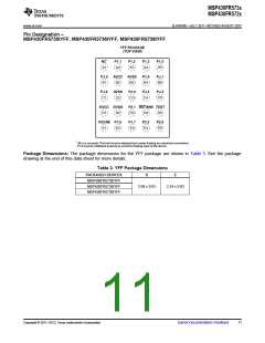
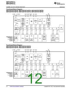
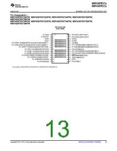
MSP430FR573x
MSP430FR572x
www.ti.com
SLAS639D –JULY 2011–REVISED AUGUST 2012
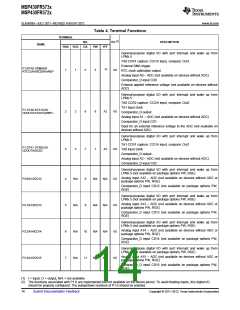
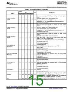
Table 4. Terminal Functions (continued)
TERMINAL
(1)
NO.
DA
I/O
DESCRIPTION
NAME
RHA RGE
PW
YFF
General-purpose digital I/O with port interrupt and wake up from
LPMx.5
TA1 CCR2 capture: CCI2A input, compare: Out2
Slave transmit enable – eUSCI_B0 SPI mode
Analog input A3 – ADC (not available on devices without ADC)
Comparator_D input CD3
P1.3/TA1.2/UCB0STE/
A3/CD3
8
4
12
8
A4
I/O
General-purpose digital I/O with port interrupt and wake up from
LPMx.5
TB0 CCR1 capture: CCI1A input, compare: Out1
Slave transmit enable – eUSCI_A0 SPI mode
Analog input A4 – ADC (not available on devices without ADC)
Comparator_D input CD4
P1.4/TB0.1/UCA0STE/
A4/CD4
9
5
13
9
B4
I/O
General-purpose digital I/O with port interrupt and wake up from
LPMx.5
TB0 CCR2 capture: CCI2A input, compare: Out2
P1.5/TB0.2/UCA0CLK/
A5/CD5
10
6
14
10
A5
I/O
Clock signal input – eUSCI_B0 SPI slave mode, Clock signal
output – eUSCI_B0 SPI master mode
Analog input A5 – ADC (not available on devices without ADC)
Comparator_D input CD5
General-purpose digital I/O
Test data output port
PJ.0/TDO/TB0OUTH/
SMCLK/CD6
11
12
7
8
15
16
11
12
C3
B5
I/O
I/O
(3)
Switch all PWM outputs high impedance input – TB0
SMCLK output
Comparator_D input CD6
General-purpose digital I/O
Test data input or test clock input
PJ.1/TDI/TCLK/TB1OUTH/
Switch all PWM outputs high impedance input – TB1 (not available
on devices without TB1)
(3)
MCLK/CD7
MCLK output
Comparator_D input CD7
General-purpose digital I/O
Test mode select
PJ.2/TMS/TB2OUTH/
ACLK/CD8
Switch all PWM outputs high impedance input – TB2 (not available
on devices without TB2)
13
14
9
17
18
13
14
C4
C5
I/O
I/O
(3)
ACLK output
Comparator_D input CD8
General-purpose digital I/O
Test clock
(3)
PJ.3/TCK/CD9
10
Comparator_D input CD9
General-purpose digital I/O with port interrupt and wake up from
LPMx.5 (not available on package options PW, RGE)
P4.0/TB2.0
P4.1
15
16
N/A
N/A
N/A
N/A
N/A
N/A
N/A
N/A
I/O
I/O
TB2 CCR0 capture: CCI0B input, compare: Out0 (not available on
devices without TB2 or package options DA, PW, RGE)
General-purpose digital I/O with port interrupt and wake up from LPMx.5 (not
available on package options DA, PW, RGE)
(3) See JTAG Operation for use with JTAG function.
Copyright © 2011–2012, Texas Instruments Incorporated
Submit Documentation Feedback
15

 TI [ TEXAS INSTRUMENTS ]