MSP430FR573x
MSP430FR572x
SLAS639D –JULY 2011–REVISED AUGUST 2012
www.ti.com
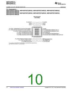
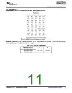
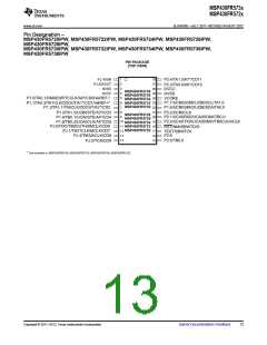
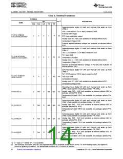
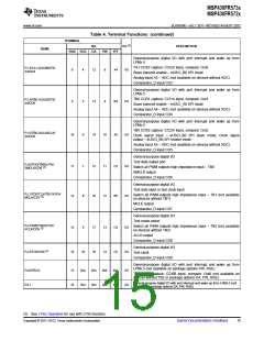
Table 4. Terminal Functions
TERMINAL
(1)
NO.
I/O
DESCRIPTION
NAME
RHA RGE
DA
PW
YFF
General-purpose digital I/O with port interrupt and wake up from
LPMx.5
TA0 CCR1 capture: CCI1A input, compare: Out1
External DMA trigger
P1.0/TA0.1/DMAE0/
RTCCLK/A0/CD0/VeREF-
(2)
1
1
5
5
I/O
RTC clock calibration output
Analog input A0 – ADC (not available on devices without ADC)
Comparator_D input CD0
External applied reference voltage (not available on devices without
ADC)
General-purpose digital I/O with port interrupt and wake up from
LPMx.5
TA0 CCR2 capture: CCI2A input, compare: Out2
TA1 input clock
P1.1/TA0.2/TA1CLK/
CDOUT/A1/CD1/VeREF+
2
2
6
6
A2
I/O
Comparator_D output
Analog input A1 – ADC (not available on devices without ADC)
Comparator_D input CD1
Input for an external reference voltage to the ADC (not available on
devices without ADC)
General-purpose digital I/O with port interrupt and wake up from
LPMx.5
TA1 CCR1 capture: CCI1A input, compare: Out1
TA0 input clock
P1.2/TA1.1/TA0CLK/
CDOUT/A2/CD2
3
3
7
7
A3
I/O
Comparator_D output
Analog input A2 – ADC (not available on devices without ADC)
Comparator_D input CD2
General-purpose digital I/O with port interrupt and wake up from
LPMx.5 (not available on package options PW, RGE)
Analog input A12 – ADC (not available on devices without ADC or
package options PW, RGE)
P3.0/A12/CD12
P3.1/A13/CD13
P3.2/A14/CD14
P3.3/A15/CD15
4
5
6
7
N/A
N/A
N/A
N/A
8
9
N/A
N/A
N/A
N/A
N/A
N/A
N/A
N/A
I/O
I/O
I/O
I/O
Comparator_D input CD12 (not available on package options PW,
RGE)
General-purpose digital I/O with port interrupt and wake up from
LPMx.5 (not available on package options PW, RGE)
Analog input A13 – ADC (not available on devices without ADC or
package options PW, RGE)
Comparator_D input CD13 (not available on package options PW,
RGE)
General-purpose digital I/O with port interrupt and wake up from
LPMx.5 (not available on package options PW, RGE)
Analog input A14 – ADC (not available on devices without ADC or
package options PW, RGE)
10
11
Comparator_D input CD14 (not available on package options PW,
RGE)
General-purpose digital I/O with port interrupt and wake up from
LPMx.5 (not available on package options PW, RGE)
Analog input A15 – ADC (not available on devices without ADC or
package options PW, RGE)
Comparator_D input CD15 (not available on package options PW,
RGE)
(1) I = input, O = output, N/A = not available
(2) The functions associated with P1.0 are implemented but not available on the device pinout. To avoid floating inputs, this digital I/O
should be properly configured. The pullup/down resistors of P1.0 should be enabled.
14
Submit Documentation Feedback
Copyright © 2011–2012, Texas Instruments Incorporated

 TI [ TEXAS INSTRUMENTS ]