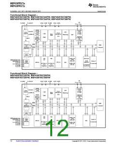
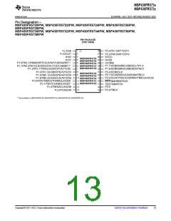
MSP430FR573x
MSP430FR572x
SLAS639D –JULY 2011–REVISED AUGUST 2012
www.ti.com
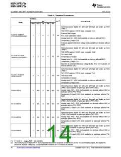
Table 4. Terminal Functions (continued)
TERMINAL
(1)
NO.
I/O
DESCRIPTION
NAME
RHA RGE
DA
PW
YFF
General-purpose digital I/O with port interrupt and wake up from
LPMx.5
P2.5/TB0.0/UCA1TXD/
UCA1SIMO
17
18
N/A
19
15
N/A
I/O
TB0 CCR0 capture: CCI0A input, compare: Out0
Transmit data – eUSCI_A1 UART mode, Slave in, master out –
eUSCI_A1 SPI mode (not available on devices without UCSI_A1)
General-purpose digital I/O with port interrupt and wake up from
LPMx.5
P2.6/TB1.0/UCA1RXD/
UCA1SOMI
TB1 CCR0 capture: CCI0A input, compare: Out0 (not available on
devices without TB1)
N/A
20
16
N/A
I/O
Receive data – eUSCI_A1 UART mode, Slave out, master in –
eUSCI_A1 SPI mode (not available on devices without UCSI_A1)
Test mode pin – enable JTAG pins
Spy-Bi-Wire input clock
(3) (4)
TEST/SBWTCK
19
20
11
12
21
22
17
18
D5
D4
I
Reset input active low
(3) (4)
RST/NMI/SBWTDIO
I/O
Non-maskable interrupt input
Spy-Bi-Wire data input/output
General-purpose digital I/O with port interrupt and wake up from
LPMx.5
TB2 CCR0 capture: CCI0A input, compare: Out0 (not available on
devices without TB2)
P2.0/TB2.0/UCA0TXD/
UCA0SIMO/TB0CLK/ACLK
21
13
23
19
E5
I/O
(4)
Transmit data – eUSCI_A0 UART mode, Slave in, master out –
eUSCI_A0 SPI mode
TB0 clock input
ACLK output
General-purpose digital I/O with port interrupt and wake up from
LPMx.5
TB2 CCR1 capture: CCI1A input, compare: Out1 (not available on
devices without TB2)
P2.1/TB2.1/UCA0RXD/
UCA0SOMI/TB0.0
22
23
24
14
24
25
26
20
D3
I/O
I/O
I/O
(5)
Receive data – eUSCI_A0 UART mode, Slave out, master in –
eUSCI_A0 SPI mode
TB0 CCR0 capture: CCI0A input, compare: Out0
General-purpose digital I/O with port interrupt and wake up from
LPMx.5
TB2 CCR2 capture: CCI2A input, compare: Out2 (not available on
devices without TB2)
P2.2/TB2.2/UCB0CLK/ TB1.0
15
21
E4
Clock signal input – eUSCI_B0 SPI slave mode, Clock signal
output – eUSCI_B0 SPI master mode
TB1 CCR0 capture: CCI0A input, compare: Out0 (not available on
devices without TB1)
General-purpose digital I/O with port interrupt and wake up from
LPMx.5 (not available on package options PW, RGE)
TB1 CCR1 capture: CCI1B input, compare: Out1 (not available on
devices without TB1)
P3.4/TB1.1/TB2CLK/ SMCLK
N/A
N/A
N/A
TB2 clock input (not available on devices without TB2 or package
options PW, RGE)
SMCLK output (not available on package options PW, RGE)
(4) See Bootstrap Loader (BSL) and JTAG Operation for use with BSL and JTAG functions.
(5) See Bootstrap Loader (BSL) and JTAG Operation for use with BSL and JTAG functions.
16
Submit Documentation Feedback
Copyright © 2011–2012, Texas Instruments Incorporated

 TI [ TEXAS INSTRUMENTS ]