ꢀ
ꢁ
ꢂ
ꢃ
ꢄ
ꢅ
ꢆ
ꢆ
ꢆꢇ ꢈ ꢁꢉ ꢊꢋꢌꢍꢉ ꢎꢏꢎꢉꢈ ꢁꢐ ꢑ ꢒꢐ ꢀꢁꢎꢓ ꢋ ꢉꢐ ꢔ ꢒꢋ ꢑꢁ ꢋꢑ
ꢇ ꢈꢁ ꢊ ꢑꢋꢓ ꢕ ꢀꢎꢁꢐ ꢑ
SLVS033F − FEBRUARY 1990 − REVISED NOVEMBER 2004
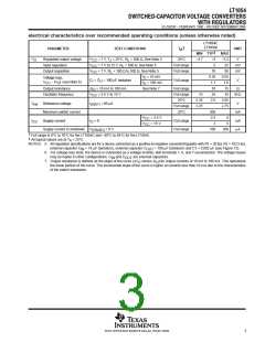
electrical characteristics over recommended operating conditions (unless otherwise noted)
LT1054C
LT1054I
†
PARAMETER
TEST CONDITIONS
UNIT
T
A
‡
MIN TYP
MAX
−5.2
25
V
O
Regulated output voltage
Input regulation
V
CC
V
CC
V
CC
= 7 V, T = 25°C, R = 500 Ω, See Note 5
25°C
−4.7
−5
5
V
J
L
= 7 V to 12 V, R = 500 Ω, See Note 5
Full range
Full range
mV
mV
L
Output regulation
= 7 V, R = 100 Ω to 500 Ω, See Note 5
10
50
L
I
= 10 mA
0.35
1.1
10
0.55
1.6
Voltage loss,
O
O
C = C = 100-µF tantalum
Full range
V
I
O
V
CC
− |V (see Note 6)
O
I
= 100 mA
Output resistance
∆I = 10 mA to 100 mA,
O
See Note 7
Full range
Full range
25°C
15
Ω
Oscillator frequency
V
CC
= 3.5 V to 15 V
15
2.35
2.25
25
35
kHz
2.5
2.65
2.75
V
ref
Reference voltage
I
= 60 µA
V
(REF)
Full range
25°C
Maximum switch current
300
2.5
3
mA
V
V
= 3.5 V
= 15 V
4
5
CC
I
Supply current
I = 0
O
Full range
Full range
mA
CC
CC
Supply current in shutdown
V
= 0 V
100
200
µA
(FB/SD)
†
‡
Full range is 0°C to 70°C for the LT1054C and −40°C to 85°C for the LT1054I.
All typical values are at T = 25°C.
A
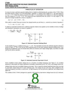
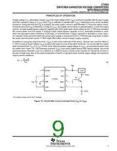
NOTES: 5. All regulation specifications are for a device connected as a positive-to-negative converter/regulator with R1 = 20 kΩ, R2 = 102.5 kΩ,
external capacitor C = 10 µF (tantalum), external capacitor C = 100 µF (tantalum) and C1 = 0.002 µF (see Figure 15).
IN OUT
6. For voltage-loss tests, the device is connected as a voltage inverter, with terminals 1, 6, and 7 unconnected. The voltage losses
may be higher in other configurations. C and C are external capacitors.
IN OUT
7. Output resistance is defined as the slope of the curve (∆V versus ∆I ) for output currents of 10 mA to 100 mA. This represents
O
O
the linear portion of the curve. The incremental slope of the curve is higher at currents less than 10 mA due to the characteristics
of the switch transistors.
3
POST OFFICE BOX 655303 • DALLAS, TEXAS 75265

 TI [ TEXAS INSTRUMENTS ]