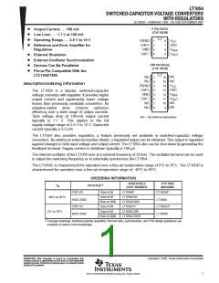
ꢀꢁ ꢂꢃ ꢄꢅ
ꢆ
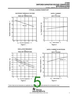
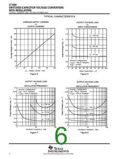
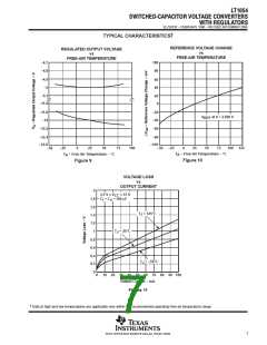
ꢇꢈ ꢁ ꢊ ꢑ ꢋꢓꢕ ꢀ ꢎꢁꢐ ꢑꢆ
ꢇ
ꢈ
ꢁ
ꢉ
ꢊ
ꢋ
ꢌ
ꢍ
ꢉ
ꢎ
ꢏ
ꢎ
ꢉ
ꢈ
ꢁ
ꢐ
ꢑ
ꢒ
ꢐ
ꢀ
ꢁ
ꢎ
ꢓ
ꢋ
ꢉ
ꢐ
ꢔ
ꢒꢋ
ꢑ
ꢁ
ꢋ
ꢑ
ꢆ
SLVS033F − FEBRUARY 1990 − REVISED NOVEMBER 2004
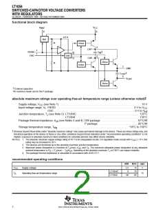
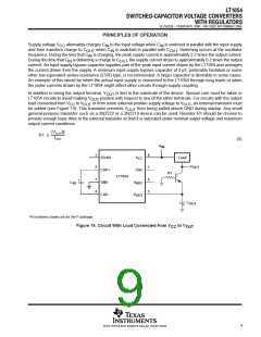
functional block diagram
V
REF
V
CC
6
8
2.5 V
Ref
R
R
Drive
Drive
2
4
+
−
CAP +
1
7
†
FB/SD
OSC
C
IN
Q
OSC
CAP −
Q
Drive
3
GND
†
C
OUT
5
V
OUT
Drive
†
External capacitors
Pin numbers shown are for the P package.
‡
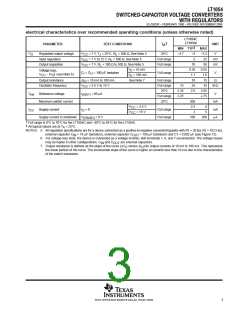
absolute maximum ratings over operating free-air temperature range (unless otherwise noted)
Supply voltage, V
(see Note 1) . . . . . . . . . . . . . . . . . . . . . . . . . . . . . . . . . . . . . . . . . . . . . . . . . . . . . . . . . . . 16 V
CC
Input voltage range, V : FB/SD . . . . . . . . . . . . . . . . . . . . . . . . . . . . . . . . . . . . . . . . . . . . . . . . . . . . . . . . 0 V to V
I
CC
OSC . . . . . . . . . . . . . . . . . . . . . . . . . . . . . . . . . . . . . . . . . . . . . . . . . . . . . . . . . . . 0 V to V
ref
Junction temperature, T (see Note 2): LT1054C . . . . . . . . . . . . . . . . . . . . . . . . . . . . . . . . . . . . . . . . . . . . . 125°C
J
LT1054I . . . . . . . . . . . . . . . . . . . . . . . . . . . . . . . . . . . . . . . . . . . . . . 135°C
Package thermal impedance, θ (see Notes 3 and 4): DW package . . . . . . . . . . . . . . . . . . . . . . . . . . 57°C/W
JA
P package . . . . . . . . . . . . . . . . . . . . . . . . . . . . 85°C/W
. . . . . . . . . . . . . . . . . . . . . . . . . . . . . . . . . . . . . . . . . . . . . . . . . . . −55°C to 150°C
Storage temperature range, T
stg
‡
Stresses beyond those listed under “absolute maximum ratings” may cause permanent damage to the device. These are stress ratings only, and
functional operation of the device at these or any other conditions beyond those indicated under “recommended operating conditions” is not
implied. Exposure to absolute-maximum-rated conditions for extended periods may affect device reliability.
NOTES: 1. The absolute maximum supply-voltage rating of 16 V is for unregulated circuits. For regulation-mode circuits with V
rating may be increased to 20 V.
≤ 15 V, this
OUT
2. The devices are functional up to the absolute maximum junction temperature.
3. Maximum power dissipation is a function of T (max), θ , and T . The maximum allowable power dissipation at any allowable
JA
J
A
ambient temperature is P = (T (max) − T )/θ . Operating at the absolute maximum T of 150°C can impact reliability.
D
J
A
JA
J
4. The package thermal impedance is calculated in accordance with JESD 51-7.
recommended operating conditions
MIN
3.5
0
MAX
15
UNIT
V
Supply voltage
V
CC
LT1054C
LT1054I
70
T
A
Operating free-air temperature range
°C
−40
85
2
POST OFFICE BOX 655303 • DALLAS, TEXAS 75265

 TI [ TEXAS INSTRUMENTS ]