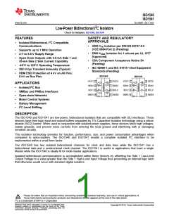
ISO1540
ISO1541
SLLSEB6 –JULY 2012
www.ti.com
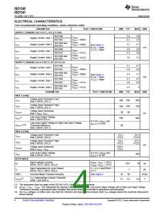
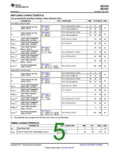
ELECTRICAL CHARACTERISTICS
Over recommended operating conditions, unless otherwise noted
PARAMETER
SUPPLY CURRENT (3V ≤ VCC1, VCC2 ≤ 3.6V)
ISO1540
TEST CONDITIONS
MIN TYP
MAX UNIT
2.4
2.1
3.6
3.3
VSDA1
VSCL1 = GND1;
VSDA2
VSCL2 = GND2
,
ICC1
ICC2
ICC1
ICC2
Supply Current, Side 1
Supply Current, Side 2
Supply Current, Side 1
Supply Current, Side 2
ISO1541
,
ISO1540 and
ISO1541
1.7
2.7
See Figure 1;
R1,R2 = Open,
C1,C2 = Open
mA
3.8
ISO1540
ISO1541
2.5
2.3
VSDA1
VSCL1 = VCC1;
VSDA2
VSCL2 = VCC2
,
3.6
,
ISO1540 and
ISO1541
1.9
3.1
SUPPLY CURRENT (4.5 V ≤ VCC1, VCC2 ≤ 5.5 V)
ISO1540
3.1
2.8
4.7
4.4
VSDA1
VSCL1 = GND1;
VSDA2
VSCL2 = GND2
,
ICC1
ICC2
ICC1
ICC2
Supply Current, Side 1
Supply Current, Side 2
Supply Current, Side 1
Supply Current, Side 2
ISO1541
,
ISO1540 and
ISO1541
2.3
3.7
See Figure 1;
R1,R2 = Open,
C1,C2 = Open
mA
4.7
ISO1540
ISO1541
3.1
2.9
VSDA1
VSCL1 = VCC1;
VSDA2
VSCL2 = VCC2
,
4.5
,
ISO1540 and
ISO1541
2.5
4
PARAMETER
TEST CONDITIONS
MIN TYP
MAX UNIT
SIDE 1 (Only)
Voltage Input Threshold “Low”,
Side 1 (SDA1, SCL1)
VILT1
500 550
540 610
660
700
Voltage Input Threshold “High”,
Side 1 (SDA1, SCL1)
VIHT1
Voltage Input Hysteresis,
Side 1 VIHT1- VILT1
VHYST1
40
60
mV
Low-Level Output Voltage,
Side 1 (SDA1,SCL1)
(1)
VOL1
650
800
0.5 mA ≤ (ISDA1 and
ISCL1) ≤ 3.5 mA
Low-Level Output Voltage to High-Level Input Voltage
Threshold Difference,
(1)(2)
ΔVOIT1
50
Side 1 (SDA1, SCL1)
SIDE 2 (Only)
Voltage Input Threshold “Low”,
Side 2 (SDA2, SCL2)
0.3 x
VCC2
0.4 x
VCC2
VILT2
Voltage Input Threshold “High”,
Side 2 (SDA2, SCL2)
0.4 x
VCC2
0.5 x
VCC2
VIHT2
mV
Voltage Input Hysteresis,
Side 2 VIHT2 - VILT2
0.05 x
VCC2
VHYST2
Low-Level Output Voltage,
Side 2 (SDA2, SCL2)
0.5 mA ≤ (ISDA2 and
ISCL2) ≤ 35 mA
VOL2
400
BOTH SIDES
Input Leakage Currents
(SDA1, SCL1, SDA2, SCL2)
VSDA1, VSCL1 = VCC1;
VSDA2, VSCL2 = VCC2
|II|
0.01
10
µA
Input Capacitance to Local Ground
(SDA1, SCL1, SDA2, SCL2)
VI = 0.4 x sin(2E6πt) +
2.5 V
CI
7
50
pF
kV/µs
V
CMTI
Common-Mode Transient Immunity
See Figure 3
25
VCC Undervoltage Lockout Threshold
(Side 1 and Side 2)
(3)
VCCUV
2.1
2.5
2.8
(1) This parameter does not apply to the ISO1541 SCL1 line as it is uni-directional.
(2) ∆VOIT1 = VOL1 – VIHT1. This represents the minimum difference between a Low-Level Output Voltage and a High-Level Input Voltage
Threshold to prevent a permanent latch condition that would otherwise exist with bi-directional communication.
(3) Any VCC voltages, on either side, less than the minimum will ensure device lockout. Both VCC voltages above the maximum will prevent
device lockout.
4
Submit Documentation Feedback
Copyright © 2012, Texas Instruments Incorporated
Product Folder Link(s): ISO1540 ISO1541

 TI [ TEXAS INSTRUMENTS ]