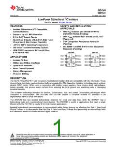
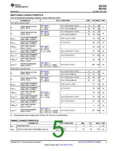
ISO1540
ISO1541
SLLSEB6 –JULY 2012
www.ti.com
These devices have limited built-in ESD protection. The leads should be shorted together or the device placed in conductive foam
during storage or handling to prevent electrostatic damage to the MOS gates.
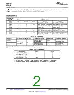
PIN FUNCTIONS
ISO1540 and
ISO1541
I / O
DESCRIPTION
NAME
VCC1
SDA1
SCL1
GND1
GND2
SCL2
SDA2
VCC2
PIN
1
ISO1540
ISO1541
ISO1540
ISO1541
-
I / O
I / O
-
-
Supply Voltage, Side 1
Supply Voltage, Side 1
2
I / O
Serial Data, Side 1 Input/Output Serial Data, Side 1 Input/Output
Serial Clock Input/Output, Side 1 Serial Clock Input, Side 1
3
I
4
-
Ground, Side 1
Ground, Side 2
Ground, Side 1
Ground, Side 2
5
-
-
O
6
I / O
I / O
-
Serial Clock Input/Output, Side 2 Serial Clock Output, Side 2
Serial Data Input/Output, Side 2 Serial Data Input/Output, Side 2
7
I / O
-
8
Supply Voltage, Side 2
Supply Voltage, Side 2
AVAILABLE OPTIONS
PRODUCT
RATED ISOLATION PACKAGE
CHANNEL DIRECTION
MARKED AS
ORDERING NUMBER
ISO1540D (rail)
ISO1540DR (reel)
ISO1541D (rail)
ISO1541DR (reel)
Both SDA and SCL
are Bidirectional
ISO1540
IS1540
4000-VPK and
2500-VRMS
D-8
(1)
SDA is Bidirectional
SCL is Unidirectional
ISO1541
IS1541
(1) See the Regulatory Information table for detailed Isolation specifications.
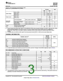
Table 1. FUNCTION TABLE(1)
POWER STATE
INPUT
OUTPUT
VCC1 or VCC2 < 2.1 V
VCC1 and VCC2 > 2.8 V
VCC1 and VCC2 > 2.8 V
VCC1 and VCC2 > 2.8 V
X
L
Z
L
Z
?
H
Z(2)
(1) H = High Level; L = Low Level; Z = High Impedance or Float; X = Irrelevant; ? = Indeterminate
(2) Invalid input condition as an I2C system requires that a pull-up resistor to VCC is connected.
2
Submit Documentation Feedback
Copyright © 2012, Texas Instruments Incorporated
Product Folder Link(s): ISO1540 ISO1541

 TI [ TEXAS INSTRUMENTS ]