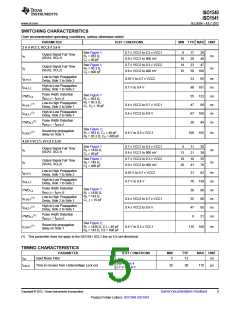
ISO1540
ISO1541
www.ti.com
SLLSEB6 –JULY 2012
(1)(2)
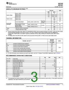
ABSOLUTE MAXIMUM RATINGS
VALUES
UNIT
MIN
–0.5
–0.5
–0.5
MAX
VCC1, VCC2
6
V
V
Supply voltage
Output current
SDA1, SCL1
SDA2, SCL2
SDA1, SCL1
SDA2, SCL2
VCC1 + 0.5
VCC2 + 0.5
V
±20
±100
±8
mA
mA
kV
Bus Pins
All Pins
Human Body Model
ESDA, JEDEC JS-001-2012
±4
Electrostatic
Discharge
Field-Induced-Charged
Device Model
JEDEC JESD22-C101E
JEDEC JESD22-A115-A
±1.5
kV
All Pins
Machine Model
±200
150
V
TJ(MAX)
TSTG
Maximum junction temperature
Storage temperature range
°C
°C
–65
150
(1) Stresses beyond those listed under ABSOLUTE MAXIMUM RATINGS cause permanent damage to the device. These are stress ratings
only and functional operation of the device at these or any other conditions beyond those indicated under RECOMMENDED
OPERATING CONDITIONS is not implied. Exposure to absolute-maximum-rated conditions for extended periods affects device
reliability.
(2) All voltage values here within are with respect to the local ground terminal (GND1 or GND2) and are peak voltage values.
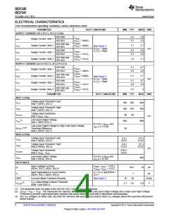
THERMAL INFORMATION
ISO1540
ISO1541
THERMAL METRIC(1)
UNITS
D (8 PINS)
114.6
69.6
θJA
Junction-to-ambient thermal resistance
θJCtop
θJB
Junction-to-case (top) thermal resistance
Junction-to-board thermal resistance
55.3
°C/W
ψJT
Junction-to-top characterization parameter
Junction-to-board characterization parameter
Junction-to-case (bottom) thermal resistance
27.2
ψJB
54.7
θJCbot
n/a
(1) For more information about traditional and new thermal metrics, see the IC Package Thermal Metrics application report, SPRA953.
RECOMMENDED OPERATING CONDITIONS
MIN
NOM
MAX
5.5
UNIT
VCC1, VCC2
Supply Voltage
3
VSDA1, VSCL1
Input/Output Signal Voltages, Side 1
Input/Output Signal Voltages, Side 2
Low-Level Input Voltage, Side 1
High-Level Input Voltage, Side 1
Low-Level Input Voltage, Side 2
High-Level Input Voltage, Side 2
Output Current, Side 1
0
VCC1
VCC2
0.5
VSDA2, VSCL2
VIL1
0
0
V
VIH1
VIL2
0.7 x VCC1
VCC1
0.3 x VCC2
VCC2
3.5
0
0.7 x VCC2
0.5
VIH2
IOL1
mA
pF
IOL2
Output Current, Side 2
0.5
35
Cb1
Maximum Capacitive Load, Side 1
Maximum Capacitive Load, Side 2
40
Cb2
400
(1)
fMAX
TA
Maximum Operating Frequency
1
MHz
°C
Ambient Temperature
Junction Temperature
Thermal Shutdown
–40
–40
139
125
TJ
136
°C
TSD
171
°C
(1) This represents the maximum frequency with the maximum bus load (Cb) and the maximum current sink (IO). If the system has less bus
capacitance, then higher frequencies can be achieved.
Copyright © 2012, Texas Instruments Incorporated
Submit Documentation Feedback
3
Product Folder Link(s): ISO1540 ISO1541

 TI [ TEXAS INSTRUMENTS ]