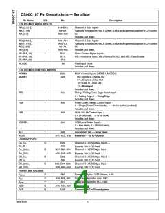
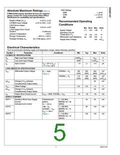
AC Timing Diagrams
30151675
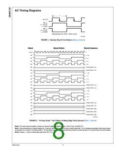
FIGURE 1. Checker Board Test Pattern (Note 6, Note 8)
30151674
FIGURE 2. “16 Gray Scale” Test Pattern (Falling Edge Clock shown) (Note 7, Note 8)
Note 6: The worst case test pattern produces a maximum toggling of digital circuits, LVDS I/O and LVCMOS/ I/O.
Note 7: Recommended pin to signal mapping for 18 bits per pixel, customer may choose to define differently. The 16 grayscale test pattern tests device power
consumption for a “typical” LCD display pattern. The test pattern approximates signal switching needed to produce groups of 16 vertical stripes across the display.
Note 8: Figures 1, 2 show a falling edge data strobe (IN_CLK).
www.ti.com
8

 TI [ TEXAS INSTRUMENTS ]