ESD Ratings:
HBM
CDM
Absolute Maximum Ratings (Note 1)
If Military/Aerospace specified devices are required,
please contact the Texas Instruments Sales Office/
Distributors for availability and specifications.
> ±8 kV
> ±1.25 kV
>±250 V
MM
Supply Voltage (VCC
)
−0.3V to +2.5V
−0.3V to VDD + 0.3V
Recommended Operating
Conditions
LVCMOS Input Voltage
LVDS Driver Output
Voltage
LVDS Output Short Circuit
Duration
Junction Temperature
Storage Temperature
Package Derating: θJA
−0.3V to +3.6V
Min Nom Max Units
Supply Voltage
1.71 1.80 1.89
V
Continuous
+150°C
−65°C to +150°C
Operating Free Air
Temperature (TA)
−10 +25 +70
°C
Differential Load Impedance
Supply Noise Voltage
100 120
80
Ω
35.1°C/W above +22°C
<90 mVp-p
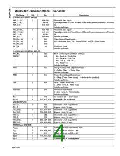
Electrical Characteristics
Over recommended operating supply and temperature ranges unless otherwise specified.
Symbol Parameter Conditions
LVCMOS DC SPECIFICATIONS
Min
Typ
Max
Units
VIH
VIL
IIN
High Level Input Voltage
Low Level Input Voltage
Input Current
0.65VDD
GND
VDD
0.35VDD
+10
V
V
VIN = 0V or VDD
=
– 10
±1
µA
1.71 V to 1.89 V
LVDS DRIVER DC SPECIFICATIONS
VOD
Differential Output Voltage
VODSEL = VIH
VODSEL = VIL
160
(320)
300
(600)
450
(900)
mV
(mVP-P
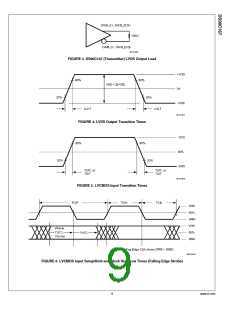
RL = 100Ω
Figure 3
)
)
110
180
300
mV
(220)
(360)
(600)
(mVP-P
Change in VOD between
Complimentary Output States
Offset Voltage
50
mV
ΔVOD
VOS
0.8
0.9
1.0
50
V
Change in VOS between
mV
ΔVOS
Complimentary Output States
Output Short Circuit Current
IOS
VOUT = GND, VODSEL = VDD
–45
−35
60
−25
85
mA
mA
SUPPLY CURRENT
IDDT1
IDDT2
IDDT3
Serializer Worst Case Supply
Current
(includes load current)
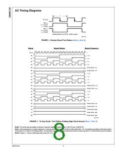
Checkerboard
pattern,
f = 105 MHz,
MODE[1:0] = 00
(SISO)
RL = 100 Ω,
18B = VIL,
f = 185 MHz,
MODE[1:0] = 01
(SIDO)
95
140
150
mA
mA
VODSEL = VIH,
VDD = 1.89 V,
Figure 1
f = 105 MHz,
MODE[1:0] = 10
(DIDO)
100
5
www.ti.com

 TI [ TEXAS INSTRUMENTS ]