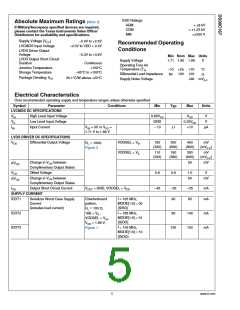
Symbol
Parameter
Conditions
Min
Typ
Max
Units
IDDTP
Serializer Supply Current PRBS-7 MODE[1:0] = 01
18B = VIL,
55
mA
(SIDO)
VODSEL = VIL,
VDD = 1.8
f = 150 MHz,
RL = 100 Ω,
PRBS-7 Pattern
Figure 12
18B = VIL,
75
49
65
53
71
48
63
18
mA
mA
mA
mA
mA
mA
mA
µA
VODSEL = VIH,
VDD = 1.8
18B = VIH,
VODSEL = VIL,
VDD = 1.8
18B = VIH,
VODSEL = VIH,
VDD = 1.8
IDDTG
Serializer Supply Current 16
Grayscale
MODE[1:0] = 01
(SIDO)
f = 150 MHz,
RL = 100 Ω,
16 Grayscale
Pattern
18B = VIL,
VODSEL = VIL,
VDD = 1.8
18B = VIL,
VODSEL = VIH,
VDD = 1.8
18B = VIH,
VODSEL = VIL,
VDD = 1.8
18B = VIH,
VODSEL = VIH,
VDD = 1.8
IDDZ
Power Down Supply Current
PDB = GND
200
Recommended Input Characteristics
Over recommended operating supply and temperature ranges unless otherwise specified.
Symbol
TCIT
Parameter
Min
1.0
Typ
Max
Units
ns
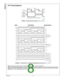
IN_CLK Transition Time
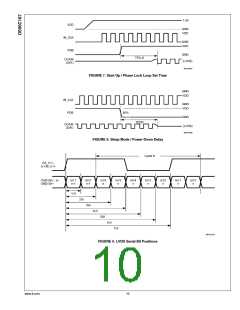
Figure 5
MODE[1:0] = 00 or 10
MODE[1:0] = 01
MODE[1:0] = 00 or 10
MODE[1:0] = 01
Figure 6
T
4.0
2.0
1.0
ns
TCIP
IN_CLK Period
Figure 6
9.53
5.40
0.35T
0.35T
1.5
T
40
ns
T
20
ns
TCIH
TCIL
TXIT
IN_CLK High Time
IN_CLK Low Time
0.5T
0.5T
0.65T
0.65T
0.3T
ns
ns
INA_x & INB_x Transition Time
Figure 5
ns
Switching Characteristics
Over recommended operating supply and temperature ranges unless otherwise specified.
Symbol
TSTC
Parameter
Min
0
Typ
Max
Units
ns
INn_x Setup to IN_CLK
INn_x Hold from IN_CLK
Figure 6
THTC
2.5
ns
LLHT
LVDS Low-to-High Transition Time
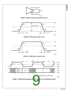
Figure 4(Note 4)
0.18
0.18
0.5
0.5
ns
LHLT
TBIT
LVDS High-to-Low Transition Time
(Note 4)
ns
LVDS Output Bit Width
MODE[1:0] = 00, or 10
MODE[1:0] = 01
1/7 TCIP
2/7 TCIP
ns
ns
www.ti.com
6

 TI [ TEXAS INSTRUMENTS ]