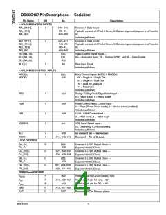
DS90C187 Pin Descriptions — Serializer
Pin Name
I/O
No.
Description
1.8V LVCMOS VIDEO INPUTS
INA_[27:21],
INA_[17:9],
INA_[8:0]
I
I
B19–B13,
B9–B1,
B40–B32
Channel A Data Inputs
Typically consists of 8 Red, 8 Green, 8 Blue and a general purpose or L/R control
bit.
Includes pull down.
INB_[27:21],
INB_[17:14],
INB_[13:9],
INB_[8:0]
A23–A17,
A10–A7,
A5–A1,
Channel B Data Inputs
Typically consists of 8 Red, 8 Green, 8 Blue and a general purpose or L/R control
bit.
A50–A42
Includes pull down.
HS (INA_18),
VS (INA_19),
DE (INA_20)
I
I
B10,
B11,
B12
Video Control Signal Inputs –
HS = Horizontal Sync, VS = Vertical SYNC, and DE = Data Enable
IN_CLK
A6
Pixel Input Clock
Includes pull down.
1.8V LVCMOS CONTROL INPUTS
MODE0,
MODE1
I
B20,
A25
Mode Control Inputs (MODE1, MODE0)
00 = Single In / Single Out
01 = Single In / Dual Out
10 = Dual In / Dual Out
11 = Reserved
Includes pull down.
RFB
I
I
I
I
A24
A40
A29
A41
Rising / Falling Clock Edge Select Input –
0 = Falling Edge, 1 = Rising Edge
Includes pull down.
PDB
Power Down (Sleep) Control Input –
0 = Sleep (Power Down mode), 1 = device active (enabled)
Includes pull down.
18B
18 bit / 24 bit Control Input –
0 = 24 bit mode, 1 = 18 bit mode
Includes pull down.
VODSEL
VOD Level Select Input –
0 = Low swing, 1 = Normal swing
Includes pull down.
N/C
I
I
A39
no connect pin — leave open
Reserved – Tie to Ground.
RSVD
A11, A12, A16
LVDS OUTPUTS
OA_C+,
OA_C-
O
O
O
O
B28,
A35
Channel A LVDS Output Clock —
Expects 100 Ω DC load.
Channel A LVDS Output Data —
Expects 100 Ω DC load.
Channel B LVDS Output Clock —
Expects 100 Ω DC load.
Channel B LVDS Output Data —
Expects 100 Ω DC load.
OA_[3:0]+,
OA_[3:0]-
B27, B29–B31
A34, A36–A38
OB_C+,
OB_C-
B23,
A30
OB_[3:0]+,
OB_[3:0]-
B21, B24–B26,
A28, A31–A33
POWER and GROUND
VDDTX
VDD
P
P
P
G
G
B22
A14, A26, A51
A13
Power supply for LVDS Drivers, 1.8V.
Power supply pin for core, 1.8V.
Power supply pin for PLL, 1.8V.
Ground pins.
VDDP
GND
DAP
A15, A27, A52
DAP
Connect DAP to Ground plane.
www.ti.com
4

 TI [ TEXAS INSTRUMENTS ]