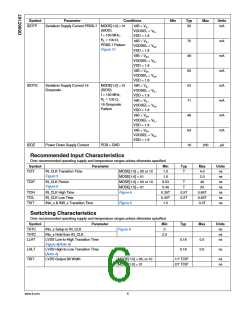
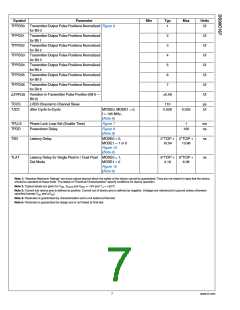
Symbol
Parameter
Min
Typ
Max
Units
TPPOS0 Transmitter Output Pulse Positions Normalized Figure 9
1
UI
for Bit 0
TPPOS1 Transmitter Output Pulse Positions Normalized
for Bit 1
2
UI
UI
UI
UI
UI
UI
UI
TPPOS2 Transmitter Output Pulse Positions Normalized
for Bit 2
3
TPPOS3 Transmitter Output Pulse Positions Normalized
for Bit 3
4
TPPOS4 Transmitter Output Pulse Positions Normalized
for Bit 4
5
6
TPPOS5 Transmitter Output Pulse Positions Normalized
for Bit 5
TPPOS6 Transmitter Output Pulse Positions Normalized
for Bit 6
7
Variation in Transmitter Pulse Position (Bit 6 —
Bit 0)
±0.06
ΔTPPOS
TCCS
TJCC
LVDS Channel to Channel Skew
Jitter Cycle-to-Cycle
110
ps
UI
MODE0, MODE1 = 0,
f = 105 MHz,
0.028
0.035
(Note 4)
TPLLS
TPDD
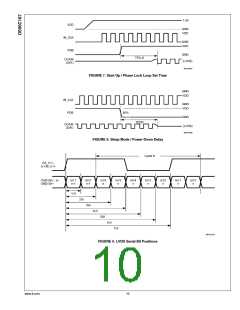
Phase Lock Loop Set (Enable Time)
Powerdown Delay
Figure 7
1
ms
ns
Figure 8
100
(Note 5)
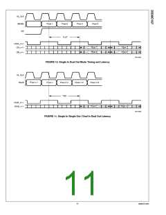
TSD
Latency Delay
MODE0 = 0,
MODE1 = 1 or 0
Figure 10
2*TCIP + 2*TCIP +
10.54 13.96
ns
(Note 4)
TLAT
Latency Delay for Single Pixel In / Dual Pixel MODE0 = 1,
9*TCIP + 9*TCIP +
4.19 6.36
ns
Out Mode
MODE1 = 0
Figure 10
(Note 4)
Note 1: “Absolute Maximum Ratings” are those values beyond which the safety of the device cannot be guaranteed. They are not meant to imply that the device
should be operated at these limits. The tables of “Electrical Characteristics” specify conditions for device operation.
Note 2: Typical values are given for VDD, VDDTX and VDDP = 1.8V and T A = +25°C.
Note 3: Current into device pins is defined as positive. Current out of device pins is defined as negative. Voltages are referenced to ground unless otherwise
specified (except VOD and ΔVOD).
Note 4: Parameter is guaranteed by characterization and is not tested at final test.
Note 5: Parameter is guaranteed by design and is not tested at final test.
7
www.ti.com

 TI [ TEXAS INSTRUMENTS ]