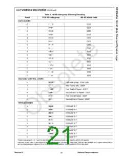
3.0 Functional Description (Continued)
3.5.4 Single 25 MHz Reference
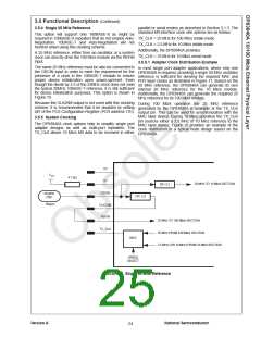
parallel or serial modes as described in Section 3.1.3. The
standard MII interface clock rate options are as follows:
This option will support only 100BASE-X as might be
required in 100BASE-X repeaters that do not employ Auto-
Negotiation. 10BASE-T and Auto-Negotiation will not
function when using this clocking scheme.
TX_CLK = 25 MHz for 100 Mb/s nibble mode
TX_CLK = 2.5 MHz for 10 Mb/s nibble mode
Additionally, the DP83840A provides:
A 25 MHz reference, either from an oscillator or a system
clock can directly drive the 100 Mb/s module via the REFIN
input.
TX_CLK = 10 MHz for 10 Mb/s serial mode
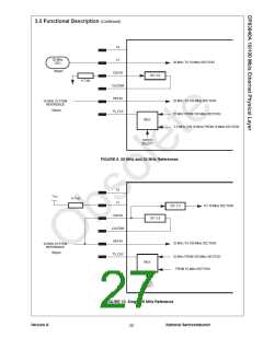
3.5.5.1 Adapter Clock Distribution Example
The same 25 MHz reference must be also be connected to
the OSCIN input in order to meet the requirement for the
presence of a clock in the 10BASE-T module to ensure
proper device initialization upon power-up/reset. Even
though the divide by 2.5 of the 25MHz clock does not yield
the typical 20MHz 10BASE-T reference, it is still sufficient
for device initialization purposes. This option is shown in
Figure 10.
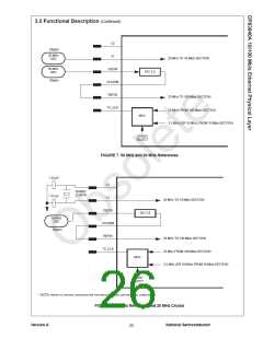
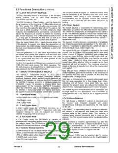
In most single port adapter applications, where only one
DP83840A is required, providing a single 50 MHz oscillator
reference is sufficient for deriving the required MAC and
PHY layer clocks as illustrated in Figure 11. Based on the
50 MHz reference, the DP83840A can generate its own
internal 20 MHz reference for the 10 Mb/s module.
Additionally, the DP83840A can generate the required 25
MHz reference for its 100 Mb/s module.
Because the CLK25M output is not used with this clocking
scheme, it is recommended that it be disabled by setting
bit7 of the PCS Configuration Register (PCR address 17h).
During 100 Mb/s operation the 25 MHz reference
generated by the DP83840A is available at the TX_CLK
output pin. This can be used for synchronization with the
MAC layer device. During 10 Mb/s operation the TX_CLK
pin sources either a 2.5 MHz or 10 MHz reference to the
MAC layer device. Figure 10 provides an example of the
clock distribution in a typical node design based on the
DP83840A.
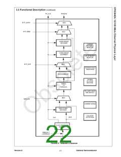
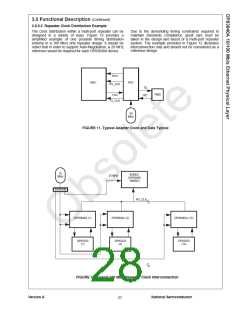
3.5.5 System Clocking
The DP83840A clock options help to simplify single port
adapter designs as well as multi-port repeaters. The
TX_CLK allows 10 Mb/s MII data to be received in either
X2
VCC
4.7 kΩ
X1
20 MHz TO 10 Mb/s SECTION
DIV 2.5
OSCIN
CLK25M
REFIN
50 MHz
OSC
DIV 2.0
50ppm
25 MHz TO 100 Mb/s SECTION
TX_CLK
25 MHz FROM 100 Mb/s SECTION
2.5 MHz (OR 10 MHz) FROM 10 Mb/s SECTION
MUX
SPEED
SELECT
FIGURE 6. Single 50 MHz Reference
Version A
National Semiconductor
24

 TI [ TEXAS INSTRUMENTS ]