3.0 Functional Description (Continued)
A remote fault is an error in the link that one station can 50ppm is recommended for all external references driving
detect while the other cannot. An example of this is a the CGM.
disconnected wire at a station’s transmitter. This station will
It is important to note that in order to provide proper device
be receiving valid data and detect that the link is good via
initialization, even when operating the DP83840A in
the Link Integrity Monitor, but will not be able to detect that
100BASE-X only mode, the 10BASE-T sections of the
its transmission is not propagating to the other station.
device must also be provided with a clock upon device
A 100BASE-FX station that detects such a remote fault power-up/reset to ensure proper device initialization. This
may modify its transmitted IDLE stream from all ones to a is taken into consideration in the following subsections.
group of 84 ones followed by a single zero (i.e. 16 IDLE
It is also important to note that the state of the internal
code groups followed by a single Data 0 code group.) This
divide-by-two flip-flop, between OSCIN and CLK25M, is
is referred to as the FEFI IDLE pattern.
unknown at power-up/reset. Therefore, the phase of
If the FEFI function has been enabled via bit 8 of the PAR CLK25M relative to that of OSCIN can be either 0 degrees
(address 19h), then the DP83840A will halt all current or 180 degrees.
operations and transmit the FEFI IDLE pattern when SD+/-
is de-asserted following a good link indication from the Link
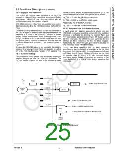
3.5.1 Single 50 MHz Reference
This option will support 10BASE-T, 100BASE-X, or
combined 10/100.
Integrity Monitor. Transmission of the FEFI IDLE pattern
will continue until SD+/- is asserted.
A 50 MHz oscillator can be used to drive the OSCIN input.
This reference is internally divided by two and then routed
to the CLK25M output pin. By connecting the CLK25M
output directly to the REFIN input pin, the 25 MHz
reference is allowed to drive the 100 Mb/s module. The 50
MHz signal is also divided by 2.5 internally to provide the
20 MHz reference directly to the 10 Mb/s module. This
option is shown in Figure 6.
If three or more FEFI IDLE patterns are detected by the
DP83840A, then bit 4 of the Basic Mode Status Register
(address 01h) is set to one until read by management.
Additionally, upon detection of Far End Fault, all receive
and transmit MII activity is disabled/ignored.
This function is optional for 100BASE-FX compliance and
should be disabled for 100BASE-TX compliance.
Note: The first FEFI IDLE pattern may contain more than 84 ones as the
pattern may have started during IDLE transmission. Also, the FEFI IDLE
pattern will not cause carrier detection.
The 10BASE-T module within the DP83840A will
automatically switch to the 20 MHz reference (sourced by
the internal 2.5 circuit) upon detection of inactivity on the
X1 input pin. When not in use, the X1 input pin should be
pulled-up to VCC (4.7 kΩ pull-up resistor recommended)).
3.4.12 Carrier Integrity Monitor
The Carrier Integrity Monitor function (CIM) protects the
repeater from transient conditions that would otherwise
cause spurious transmission due to a faulty link. This
function is required for repeater applications and is not
specified for node applications.
It should be noted that an external 20 MHz reference
driving the X1 input will provide the best over all transmit
jitter performance from the integrated 10BASE-T
transmitter.
The REPEATER pin (pin # 47) determines the default state
of bit 5 of the PCR (Carrier Integrity Monitor Disable,
address 17h) to automatically enable or disable the CIM
function as required for IEEE 802.3u/D5 compliant
applications. After power-up/hardware reset, software may
enable or disable this function independent of repeater or
node/switch mode.
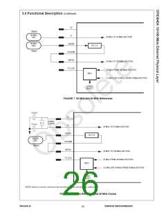
3.5.2 50 MHz and 20 MHz References
This option will support 10BASE-T, 100BASE-X, or
combined 10/100.
For improved jitter performance in the 10 Mb/s module, an
external 20 MHz oscillator can be used to drive the X1 pin.
Alternatively, a 20 MHz crystal network can be connected
across pins X1 and X2 to provide the required reference for
the 10 Mb/s module. The 100 Mb/s module must still
receive a 25 MHz reference which can be provided by a 50
MHz oscillator as described in 3.5.1. This option is shown
in Figure 7 (20 MHz oscillator module) and Figure 8 (20
MHz crystal).
If the CIM determines that the link is unstable, the
DP83840A will not propagate the received data or control
signaling to the MII and will ignore data transmitted via the
MII. The DP83840A will continue to monitor the receive
stream for valid carrier events.
Detection of an unstable link condition will cause bit 5 of
the PAR (address 19h) to be set to one. This bit is cleared
to zero upon a read operation once a stable link condition
is detected by the CIM. Upon detection of a stable link, the
DP83840A will resume normal operations.
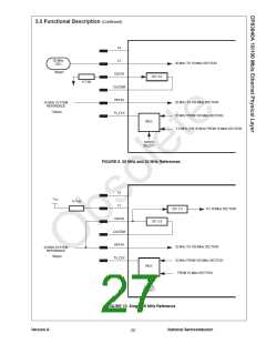
3.5.3 25 MHz and 20 MHz References
This option will support 10BASE-T, 100BASE-X, or
combined 10/100.
A 25 MHz reference, either from an oscillator or a system
clock can directly drive the 100 Mb/s module via the REFIN
input.
The Disconnect Counter (address 12h) increments each
time the CIM determines that the link is unstable.
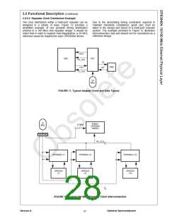
3.5 CLOCK GENERATION MODULE
A separate 20 MHz reference from either an oscillator or a
The Clock Generation Module (CGM) within the DP83840A crystal network must be provided to the X1 and X2 inputs
can be configured for several different applications. This as described in 3.5.2. This option is shown in Figure 9.
offers the flexibility of selecting a clocking scheme that is
best suited for a given design.
Because the CLK25M output is not used with this clocking
scheme, it is recommended that it be disabled by setting bit
This section describes the operation of the CGM from both 7 of the PCS Configuration Register (PCR address 17h).
the device perspective as well as at the system level such
as in an adapter or repeater. A tolerance of no greater than
Version A
National Semiconductor
23

 TI [ TEXAS INSTRUMENTS ]