DM385, DM388
SPRS821D –MARCH 2013–REVISED DECEMBER 2013
3.3.23 USB
www.ti.com
3.3.23.1 USB0
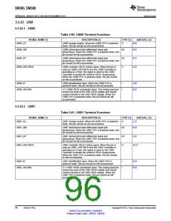
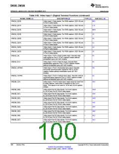
Table 3-50. USB0 Terminal Functions
SIGNAL NAME [1]
DESCRIPTION [2]
TYPE [3]
AAR BALL [4]
B20
USB0_CE
USB0_DM
USB0 charger enable. When the USB0 PHY is powered
down, this pin should be left unconnected.
O
USB0 bidirectional data differential signal pair
[plus/minus]. When the USB0 PHY is powered down, this
pin should be left unconnected.
I/O
I/O
O
B21
A21
K23
USB0_DP
USB0 bidirectional data differential signal pair
[plus/minus]. When the USB0 PHY is powered down, this
pin should be left unconnected.
USB0_DRVVBUS
USB0 Contoller VBUS Control ouput. When this pin is
used as USB0_DRVVBUS and the USB0 Controller is
operating as a Host, this signal is used by the USB0
Controller to enable the external VBUS charge pump.
When the USB0 PHY is powered down, this pin should
be left unconnected.
USB0_ID
USB0 identification input. When the USB0 PHY is
powered down, this pin should be left unconnected.
I
I
A20
B22
USB0_VBUSIN
5-V USB0 VBUS comparator input. This analog input pin
senses the level of the USB VBUS voltage and should
connect directly to the USB VBUS voltage. When the
USB0 PHY is powered down, this pin should be left
unconnected.
3.3.23.2 USB1
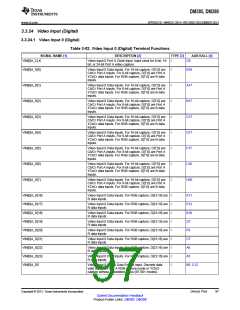
Table 3-51. USB1 Terminal Functions
SIGNAL NAME [1]
DESCRIPTION [2]
TYPE [3]
AAR BALL [4]
USB1_CE
USB1_DM
USB1 charger enable. When the USB1 PHY is powered
down, this pin should be left unconnected.
O
C21
USB1 bidirectional data differential signal pair
[plus/minus]. When the USB1 PHY is powered down, this
pin should be left unconnected.
I/O
I/O
O
B23
USB1_DP
USB1 bidirectional data differential signal pair
[plus/minus]. When the USB1 PHY is powered down, this
pin should be left unconnected.
A23
USB1_DRVVBUS
USB1 Contoller VBUS Control ouput. When this pin is
used as USB1_DRVVBUS and the USB1 Controller is
operating as a Host, this signal is used by the USB1
Controller to enable the external VBUS charge pump.
When the USB1 PHY is powered down, this pin should
be left unconnected.
AF31
USB1_ID
USB1 identification input. When the USB1 PHY is
powered down, this pin should be left unconnected.
I
I
A24
B24
USB1_VBUSIN
5-V USB1 VBUS comparator input. This analog input pin
senses the level of the USB VBUS voltage and should
connect directly to the USB VBUS voltage. When the
USB1 PHY is powered down, this pin should be left
unconnected.
96
Device Pins
Copyright © 2013, Texas Instruments Incorporated
Submit Documentation Feedback
Product Folder Links: DM385 DM388

 TI [ TEXAS INSTRUMENTS ]