DM385, DM388
SPRS821D –MARCH 2013–REVISED DECEMBER 2013
www.ti.com
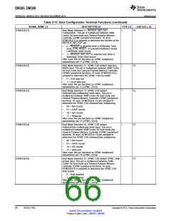
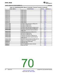
Table 3-13. Boot Configuration Terminal Functions (continued)
SIGNAL NAME [1]
DESCRIPTION [2]
TYPE [3]
AAR BALL [4]
BTMODE[11]
Boot Mode Selection 11. RSTOUT_WD_OUT
Configuration. This pin is multiplexed between ARM
Cortex-A8 boot mode and General-Purpose Memory
Controller (GPMC) peripheral functions. At reset,
BTMODE[11] is sampled to determine the function of the
RSTOUT_WD_OUT pin:
I
R4
•
0 = RSTOUT is asserted when a Watchdog Timer
reset, POR, RESET, or Emulation/Software-Global
Cold/Warm reset occurs
•
1 = RSTOUT_WD_OUT is asserted only when a
Watchdog Timer reset occurs
After reset, this pin functions as GPMC multiplexed
data/address pin 11 (GPMC_D[11]).
BTMODE[12]
Boot Mode Selection 12. GPMC CS0 default Data Bus
Width input. This pin is multiplexed between ARM Cortex-
A8 boot mode and General-Purpose Memory Controller
(GPMC) peripheral functions. At reset, BTMODE[12] is
sampled to determine the GPMC CS0 bus width:
I
R3
•
•
0 = 8-bit data bus
1 = 16-bit data bus
After reset, this pin functions as GPMC multiplexed
data/address pin 12 (GPMC_D[12]).
BTMODE[13]
Boot Mode Selection 13. GPMC CS0 default
I
R2
Address/Data multiplexing mode input. This pin is
multiplexed between ARM Cortex-A8 boot mode and
General-Purpose Memory Controller (GPMC) peripheral
functions. At reset, BTMODE[14:13] are sampled to
determine the GPMC CS0 Address/Data multiplexing:
•
•
•
•
00 = Not muxed
01 = A/A/D muxed
10 = A/D muxed
11 = Reserved
After reset, this pin functions as GPMC multiplexed
data/address pin 13 (GPMC_D[13]).
BTMODE[14]
Boot Mode Selection 14. GPMC CS0 default
I
R1
Address/Data multiplexing mode input. This pin is
multiplexed between ARM Cortex-A8 boot mode and
General-Purpose Memory Controller (GPMC) peripheral
functions. At reset, BTMODE[14:13] are sampled to
determine the GPMC CS0 Address/Data multiplexing:
•
•
•
•
00 = Not muxed
01 = A/A/D muxed
10 = A/D muxed
11 = Reserved
After reset, this pin functions as GPMC multiplexed
data/address pin 14 (GPMC_D[14]).
BTMODE[15]
Boot Mode Selection 15. GPMC CS0 default GPMC_Wait
enable input. This pin is multiplexed between ARM
Cortex-A8 boot mode and General-Purpose Memory
Controller (GPMC) peripheral functions. At reset,
BTMODE[15] is sampled to determine the GPMC CS0
Wait enable:
I
P2
•
0 = Wait disabled
•
1 = Wait enabled
After reset, this pin functions as GPMC multiplexed
data/address pin 15 (GPMC_D[15]).
66
Device Pins
Copyright © 2013, Texas Instruments Incorporated
Submit Documentation Feedback
Product Folder Links: DM385 DM388

 TI [ TEXAS INSTRUMENTS ]