DM385, DM388
www.ti.com
SPRS821D –MARCH 2013–REVISED DECEMBER 2013
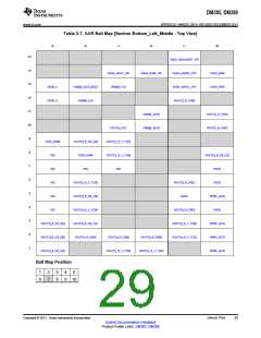
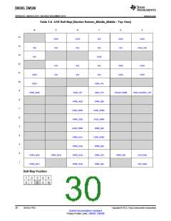
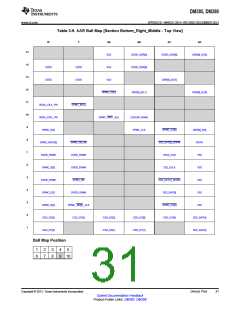
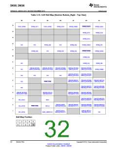
3.2 Pin Assignments
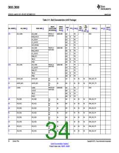
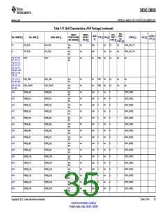
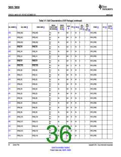
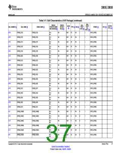
The following table provides a summary of the device signal ball assignments and characteristics.
1. BALL NUMBER: Package ball number(s) associated with each signal(s).
2. BALL NAME: The name of the package ball or terminal.
Note: The table does not take into account subsystem terminal multiplexing options.
3. SIGNAL NAME: The signal name for that ball in the mode being used.
4. PINCNTL REGISTER NAME AND ADDRESS: The name and address of the register that controls the
pin’s internal pull-up/down resistors and multiplexing options.
5. PINCNTL DEFAULT VALUE: The default value of the PINCNTL after reset.
6. MODE: The setting of the MUXMODE[10:0] bits in the associated PINCNTL register that selects this
multiplexed signal option.
7. TYPE: Signal direction
–
–
–
–
–
–
–
–
I = Input
O = Output
I/O = Input/Output
D = Open drain
DS = Differential
A = Analog
PWR = Power
GND = Ground
8. DSIS: The deselected input state (DSIS) indicates the state driven on the peripheral input (logic "0",
logic "1", or "PIN" level) when the peripheral pin function is not selected by any of the PINCNTLx
registers.
–
–
–
0: Logic 0 driven on the peripheral's input signal port.
1: Logic 1 driven on the peripheral's input signal port.
PIN: The value on the pin is driven to the peripheral's input signal port.
9. BALL RESET STATE: The state of the ball during device reset.
–
0: The buffer drives VOL (pulldown/pullup resistor not activated)
0(PD): The buffer drives VOL with an active pulldown resistor
1: The buffer drives VOH (pulldown/pullup resistor not activated)
1(PU): The buffer drives VOH with an active pullup resistor
Z: High-impedance.
–
–
–
–
L: High-impedance with an active pulldown resistor
H : High-impedance with an active pullup resistor
10. BALL RESET REL. STATE: The state of the ball following the device coming out of reset.
–
0: The buffer drives VOL (pulldown/pullup resistor not activated)
0(PD): The buffer drives VOL with an active pulldown resistor
1: The buffer drives VOH (pulldown/pullup resistor not activated)
1(PU): The buffer drives VOH with an active pullup resistor
Z: High-impedance.
–
–
–
–
L: High-impedance with an active pulldown resistor
H : High-impedance with an active pullup resistor
11. POWER: The voltage supply that powers the terminal’s I/O buffers.
12. HYS: Indicates if the input buffer is with hysteresis.
13. BUFFER TYPE: Drive strength of the associated output buffer.
Copyright © 2013, Texas Instruments Incorporated
Submit Documentation Feedback
Device Pins
33
Product Folder Links: DM385 DM388

 TI [ TEXAS INSTRUMENTS ]