DM385, DM388
SPRS821D –MARCH 2013–REVISED DECEMBER 2013
www.ti.com
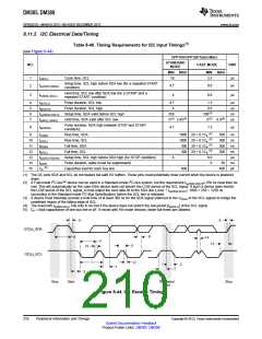
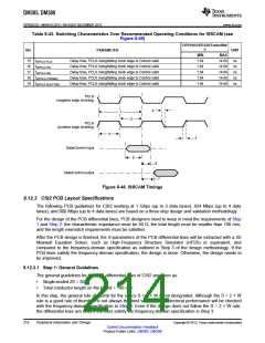
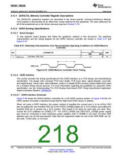
Table 8-43. Switching Characteristics Over Recommended Operating Conditions for ISSCAM (see
Figure 8-46)
OPP100/OPP120/Turbo/Nitr
o
NO.
PARAMETER
UNIT
MIN
1.64
1.64
1.64
1.64
1.64
MAX
14.68
14.68
14.68
14.68
14.68
15 td(PCLK-FLD)
16 td(PCLK-VS)
Delay time, PCLK rising/falling clock edge to Control valid
Delay time, PCLK rising/falling clock edge to Control valid
Delay time, PCLK rising/falling clock edge to Control valid
Delay time, PCLK rising/falling clock edge to Control valid
Delay time, PCLK rising/falling clock edge to Control valid
ns
ns
ns
ns
ns
17 td(PCLK-HS)
18 td(PCLK-STROBE)
19 td(PCLK-SHUTTER)
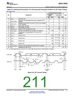
PCLK
(negative edge clocking)
4
1
3
PCLK
(positive edge clocking)
2
4
Data/Control input
Data/Control output
5
6
7
Figure 8-46. ISSCAM Timings
8.12.3 CSI2 PCB Layout Specifications
The following PCB guidelines for CSI2 working at 1 Gbps (up to 3 data lanes), 824 Mbps (up to 4 data
lanes), and 800 Mbps (up to 4 data lanes) are based on a three-step design and validation methodology.
For the design of the PCB differential lines, PCB designers need to keep in mind the requirements of Step
1 and Step 2: the characteristic impedance must be 50 Ω, the total length must be smaller than 100 mm,
and the length mismatch requirements must be satisfied.
After the PCB design is finished, the S-parameters of the PCB differential lines will be extracted with a 3D
Maxwell Equation Solver, such as High-Frequency Structure Simulator (HFSS) or equivalent, and
compared to the frequency-domain specification as outlined in Step 3 of the design methodology. If the
PCB lines satisfy the frequency-domain specification, the design is done. Otherwise, the design needs to
be improved.
8.12.3.1 Step 1: General Guidelines
The general guidelines for the PCB differential lines of CSI2 are given as:
•
•
Single-ended Z0 = 50 Ω
Total conductor length on the board < 100 mm
In this step, the general rule of thumb for the space S = 2 × W is not designated. Although the S = 2 × W
rule is a good rule of thumb, it is not always the best solution. The electrical performance will be checked
with the frequency-domain specification in Step 3. Even if the design does not follow the S = 2 × W rule,
the differential lines are okay if the lines satisfy the frequency-domain specification in Step 3.
214
Peripheral Information and Timings
Copyright © 2013, Texas Instruments Incorporated
Submit Documentation Feedback
Product Folder Links: DM385 DM388

 TI [ TEXAS INSTRUMENTS ]