DM385, DM388
www.ti.com
SPRS821D –MARCH 2013–REVISED DECEMBER 2013
8.12.1 ISS Peripheral Register Description
The ISS peripheral registers are described in the device-specific Technical Reference Manual. Each
register is documented as an offset from a base address for the peripheral. The base addresses for all of
the peripherals are in the device memory map (see Section 2.10).
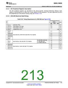
8.12.2 ISSCAM Electrical Data/Timing
Table 8-42. Timing Requirements for ISSCAM (see Figure 8-46)
OPP100/OPP120/Turb
N
O.
o/Nitro
MIN NOM
6.17
UNIT
MAX
1
2
3
4
tc(PCLK)
tw(PCLKH)
tw(PCLKL)
tt(PCLK)
Cycle time, PCLK
ns
ns
ns
Pulse duration, PCLK high
Pulse duration, PCLK low
Transition time, PCLK
2.78
2.78
2.64 ns
tsu(DATA-
PCLK)
3.11
ns
tsu(DE-PCLK)
3.11
3.11
3.11
ns
ns
ns
5
tsu(VS-PCLK) Input setup time, Data/Control valid before PCLK high/low
tsu(HS-PCLK)
tsu(FLD-
PCLK)
3.11
-0.5
0.0
ns
ns
ns
≤ 148.5 MHz clock rate
th(PCLK-
DATA)
Input hold time, Data valid after PCLK high/low
> 148.5 MHz and
≤ 162 MHz clock rate
th(PCLK-DE)
-0.5
-0.5
-0.5
-0.5
ns
ns
ns
ns
6
th(PCLK-VS)
Input hold time, Control valid after PCLK high/low
th(PCLK-HS)
th(PCLK-FLD)
Copyright © 2013, Texas Instruments Incorporated
Peripheral Information and Timings
213
Submit Documentation Feedback
Product Folder Links: DM385 DM388

 TI [ TEXAS INSTRUMENTS ]