DLPA2000
www.ti.com.cn
ZHCSCO5B –JUNE 2014–REVISED FEBRUARY 2018
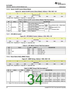
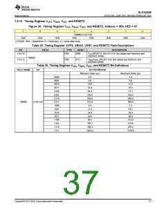
7.5.15 Timing Register VOFS, VBIAS, VRST, and RESETZ
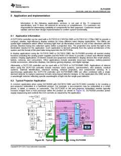
Figure 30. Timing Register VOFS, VBIAS, VRST, and RESETZ, Address = 0Eh, HEX = 07
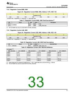
7
6
5
4
3
2
1
0
TIMING [119:112]
R/W
R/W
R/W
R/W
R/W
R/W
R/W
R/W
LEGEND: R/W = Read/Write; R = Read only; -n = value after reset.
Table 25. Timing Register VOFS, VBIAS, VRST, and RESETZ Field Descriptions
BIT
FIELD
TYPE
R/W
RESET
0000
DESCRIPTION
119:116
VOFS/RESETZ_DELAY<3:0> (for values see minimum and
maximum delay)
TIMING
115:112
R/W
0111
VBIAS/VRST_DELAY<3:0> (for values see minimum and
maximum delay)
Table 26. Timing Register VOFS, VBIAS, VRST, and RESETZ Bit Definitions
FIELD NAME
BIT
BIT DEFINITION
Minimum Delay (μs)
Maximum Delay (μs)
0000
0001
0010
0011
0100
0101
0110
0111
1000
1001
1010
1011
1100
1101
1110
1111
4.0
8.0
4.4
8.9
16.0
32.0
64.0
128.0
256.0
512.0
6.2
17.8
35.5
71.1
142.2
284.4
569.0
7.1
TIMING
[119:112]
12.4
24.9
49.8
99.5
199.1
398.3
1024.2
14.2
28.4
56.9
113.8
227.6
455.2
1138.0
Copyright © 2014–2018, Texas Instruments Incorporated
37

 TI [ TEXAS INSTRUMENTS ]