DLPA2000
ZHCSCO5B –JUNE 2014–REVISED FEBRUARY 2018
www.ti.com.cn
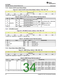
7.5.10 Switch On/Off Control (Direct Mode)
Figure 25. Switch On/Off Control (Direct Mode), Address = 09h, HEX = 00
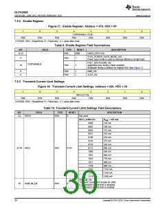
7
6
5
4
3
2
1
0
SWCNTRL [79:72]
R/W R/W
R/W
R/W
R/W
R/W
R/W
R/W
LEGEND: R/W = Read/Write; R = Read only; -n = value after reset.
Table 20. Switch On/Off Control (Direct Mode) Field Descriptions
BIT
FIELD
TYPE
RESET
DESCRIPTION
SW6 (controls switch 6 if direct mode
(see reg 11h) is enabled)
79
R/W
0
0
0
00000
00001
.....
11110
11111
2.3 V (minimum value – default value)
2.37 V
Step approximately 70 mV
4.43 V
SW5 (controls switch 5 if direct mode
(see reg 11h) is enabled)
78
R/W
SWCNTRL
SW4 (controls switch 4 if direct mode
(see reg 11h) is enabled)
77
R/W
R/W
4.5 V (maximum value)
76:72
00000
UVLO_TRIM<4:0>
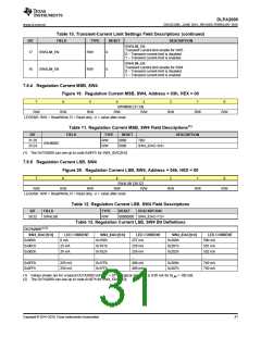
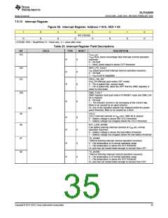
7.5.11 AFE (MUX) Control
Figure 26. AFE (MUX) Control, Address = 0Ah, HEX = 00
7
6
5
4
3
2
1
0
AFE [87:80]
R/W
R/W
R/W
R/W
R/W
R/W
R/W
R/W
LEGEND: R/W = Read/Write; R = Read only; -n = value after reset.
Table 21. AFE (MUX) Control Field Descriptions
BIT
87
FIELD
TYPE
R/W
RESET
00
DESCRIPTION
AFE_EN
86
R/W
R/W
R/W
00
00
00
AFE_CAL_DIS
AFE_GAIN<1:0>
AFE_SEL<3:0>
AFE
85:84
83:80
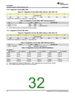
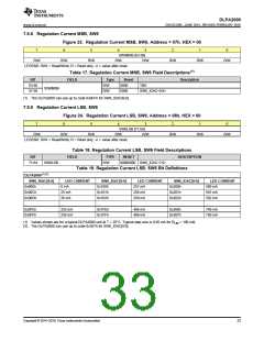
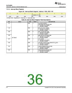
7.5.12 Break Before Make (BBM) Timing
Figure 27. BBM Timing, Address = 0Bh, HEX = 00
7
6
5
4
3
2
1
0
BBM [95:88]
R/W
R/W
R/W
R/W
R/W
R/W
R/W
R/W
LEGEND: R/W = Read/Write; R = Read only; -n = value after reset.
Table 22. BBM Timing Field Descriptions(1)
BIT
FIELD
TYPE
R/W
RESET
00000000
DESCRIPTION
95:88 BBM
BBM_DELAY<7:0>
0x00 – 0 ns
0x40 – 7326 ns
0x41 – 7437 ns
0x42 – 7548 ns
...
0x80 – 14430 ns 0xC0 – 21534 ns
0x81 – 14541 ns 0xC1 – 21645 ns
0x82 – 14652 ns 0xC2 – 21756 ns
0x01 – 333 ns
0x02 – 444 ns
...
...
...
0x3E – 7104 ns
0x3F – 7215 ns
0x7E – 14208 ns 0xBE – 21312 ns 0xFE – 28416 ns
0x7F – 14319 ns 0xBF – 21423 ns 0xFF – 28527 ns
(1) It takes 333 to 444 ns to turn off the switches from the time a change occurs on LED_SEL[1:0].
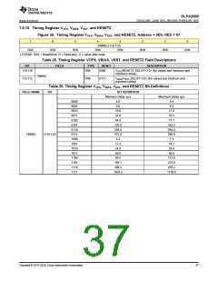
34
Copyright © 2014–2018, Texas Instruments Incorporated

 TI [ TEXAS INSTRUMENTS ]