DLPA2000
ZHCSCO5B –JUNE 2014–REVISED FEBRUARY 2018
www.ti.com.cn
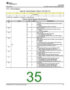
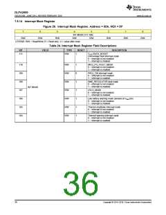
7.5.14 Interrupt Mask Register
Figure 29. Interrupt Mask Register, Address = 0Dh, HEX = DF
7
6
5
4
3
2
1
0
INT MASK [111:104]
R/W R/W
R/W
R/W
R/W
R/W
R/W
R/W
LEGEND: R/W = Read/Write; R = Read only; -n = value after reset.
Table 24. Interrupt Mask Register Field Descriptions
BIT
FIELD
TYPE
R/W
RESET
DESCRIPTION
111
1
VLED BUCK_BOOST
Overvoltage fault interrupt mask
0 – Interrupt is not masked
1 – Interrupt is masked
110
109
108
107
106
105
104
R/W
R/W
R/W
R/W
R/W
R/W
R/W
1
0
1
1
1
1
1
IREG_PG_FAULT_MASK
0 – Interrupt is not masked
1 – Interrupt is masked
PROJ_ON interrupt mask
0 – Interrupt is not masked
1 – Interrupt is masked
DMD_REGULATOR fault mask
0 – Interrupt is not masked
1 – Interrupt is masked
INT MASK
UVLO_MASK
0 – Interrupt is not masked
1 – Interrupt is masked
Low battery warning mask (sensed at VINA pin)
0 – Interrupt is not masked
1 – Interrupt is masked
Thermal shutdown interrupt mask
0 – Interrupt is not masked
1 – Interrupt is masked
Thermal warning interrupt mask
0 – Interrupt is not masked
1 – Interrupt is masked
36
Copyright © 2014–2018, Texas Instruments Incorporated

 TI [ TEXAS INSTRUMENTS ]