DAC8571
www.ti.com
SLAS373A–DECEMBER 2002–REVISED JULY 2003
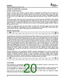
THEORY OF OPERATION (continued)
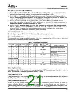
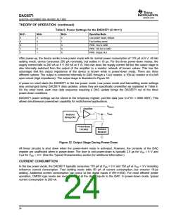
Table 6. Power Settings for the DAC8571 (C<0>=1)
M<7>
M<6>
M<5>
Operating Mode
0
0
0
1
1
0
0
1
0
1
0
Low power mode, default
Fast settling mode
PWD. 1kΩ to GND
PWD. 100 kΩ to GND
PWD. Output Hi-Z
1
X
X
X
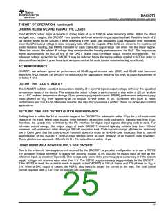
After power-up, the device works in low power mode with its normal power consumption of 170 µA at 5 V. At fast
settling mode, device consumes 250 µA nominally, but settles in 10 µs. For the three power-down modes, the
supply current falls to 200 nA at 5 V (50 nA at 3 V). Not only does the supply current fall but the output stage is
also internally switched from the output of the amplifier to a resistor network of known values. This has the
advantage that the output impedance of the device is known while in power-down mode. There are three
different options: The output is connected internally to GND through a 1-kΩ resistor, a 100-kΩ resistor or it is left
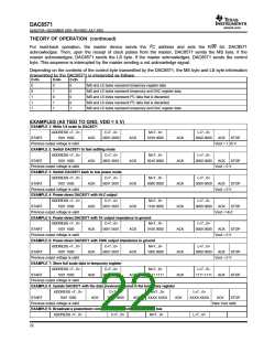
open-circuit (high impedance). The output stage is illustrated in Figure 32.
A power on reset starts the DAC8571 in the low power mode. Low power mode and fast-settling mode settings
stay unchanged during DAC8571 data updates, unless they are specifically overwritten as explained in Table 6.
On the other hand, each new data sequence requiring a DAC update brings the DAC8571 out of the three
power-down conditions.
DAC8571 power settings can be stored in the temporary register, just like data (use C<7:0> = 0000 0001). This
allows simultaneous powerdown capability for multichannel applications.
V
Sense
Amplifier
_
V
OUT
Resistor
String DAC
+
Powerdown
Circuitry
Resistor
Network
Figure 32. Output Stage During Power-Down
All linear circuitry is shut down when the power-down mode is activated. However, the contents of the DAC
register are unaffected when in power-down. The time to exit power-down is typically 2.5 µs for VDD = 5 V and
5 µs for VDD = 3 V. (See the Typical Characteristics section for additional information.)
CURRENT CONSUMPTION
In the low power mode, the DAC8571 typically consumes 170 µA at VDD = 5 V and 150 µA at VDD = 3 V including
reference current consumption. Fast settling mode adds 80 µA of current consumption, but ensures 10-µs
settling. Additional current consumption can occur at the digital inputs if VIH<<VDD. For most efficient power
operation, CMOS logic levels are recommended at the digital inputs to the DAC. In power-down mode, typical
current consumption is 200 nA.
24

 TI [ TEXAS INSTRUMENTS ]