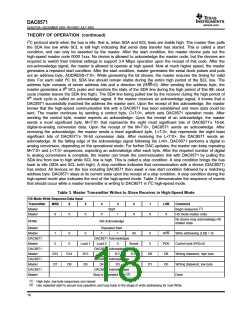
DAC8571
www.ti.com
SLAS373A–DECEMBER 2002–REVISED JULY 2003
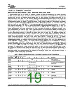
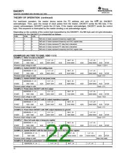
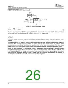
THEORY OF OPERATION (continued)
For read-back operation, the master device sends the I2C address and sets the R/W bit. DAC8571
acknowledges. Then, upon the receipt of clock pulses from the master, DAC8571 sends the MS byte. If the
master acknowledges, DAC8571 sends the LS byte. If the master acknowledges, DAC8571 sends the control
byte. This sequence is interrupted by the master sending a not acknowledge signal.
Depending on the contents of the control byte transmitted by the DAC8571, the MS byte and LS byte information
(transmitted by the DAC8571) is interpreted as follows:
C<5>
C<4>
C<2>
0
0
1
1
1
0
1
0
1
1
0
0
0
0
1
MS and LS bytes represent temporary register data
MS and LS bytes represent temporary and DAC register data
MS and LS bytes represent I2C data that is discarded
MS and LS bytes represent I2C data that is discarded
MS and LS bytes represent temporary and DAC register data
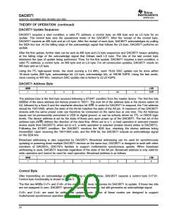
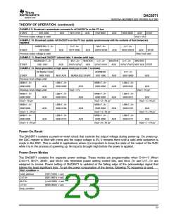
EXAMPLES (A0 TIED TO GND, VDD = 5 V)
EXAMPLE 1: Write 1/4 scale to DAC8571
ADDRESS <7...0>
1001 1000
C<7...0>
M<7...0>
L<7...0>
START
ACK
0001 0000
ACK
ACK
ACK
ACK
0100 0000
ACK
ACK
ACK
ACK
ACK
ACK
ACK
ACK
0000 0000
ACK
STOP
Previous output voltage is valid
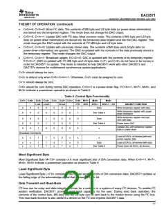
EXAMPLE 2: Switch DAC8571 to fast settling mode
Vout = 1.25 V
ADDRESS <7...0>
1001 1000
C<7...0>
M<7...0>
L<7...0>
START
ACK
0001 0001
0010 0000
0000 0000
ACK
STOP
Previous output voltage is valid
EXAMPLE 3: Switch DAC8571 back to low power mode
Vout = 0 V
ADDRESS <7...0>
1001 1000
C<7...0>
M<7...0>
L<7...0>
START
ACK
0001 0001
0000 0000
0000 0000
ACK
STOP
Previous output voltage is valid
EXAMPLE 4: Power-down DAC8571 with Hi-Z output
Vout = 0 V
ADDRESS <7...0>
1001 1000
C<7...0>
M<7...0>
L<7...0>
START
ACK
0001 0001
1100 0000
0000 0000
ACK
STOP
Previous output voltage is valid
EXAMPLE 5: Power-down DAC8571 with 1K output impedance to ground
Vout = Hi-Z
ADDRESS <7...0>
1001 1000
C<7...0>
M<7...0>
L<7...0>
START
ACK
0001 0001
ACK
0100 0000
0000 0000
ACK
STOP
Previous output voltage is valid
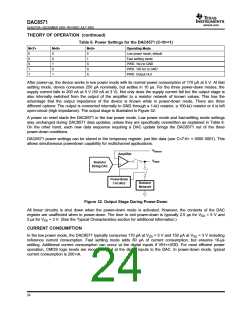
EXAMPLE 6: Power-down DAC8571 with 100K output impedance to ground
Vout = 0 V
ADDRESS <7...0>
1001 1000
C<7...0>
M<7...0>
L<7...0>
START
ACK
0001 0001
ACK
ACK
1000 0000
0000 0000
ACK
STOP
Previous output voltage is valid
EXAMPLE 7: Store full scale data in temporary register
Vout = 0 V
ADDRESS <7...0>
1001 1000
C<7...0>
M<7...0>
L<7...0>
START
ACK
0000 0000
1111 1111
1111 1111
ACK
STOP
Previous output voltage is valid
EXAMPLE 8: Update DAC8571 with the data previously stored in the temporary register
ADDRESS <7...0>
1001 1000
C<7...0>
M<7...0>
L<7...0>
START
ACK
0010 0000
ACK
XXXX XXXX
XXXX XXXX
ACK
STOP
Previous output voltage is valid
EXAMPLE 9: Broadcast a powerdown command to all DAC8571s on the I2C bus
ADDRESS <7...0> C<7...0> M<7...0>
New Vout valid
L<7...0>
22

 TI [ TEXAS INSTRUMENTS ]