DAC8571
www.ti.com
SLAS373A–DECEMBER 2002–REVISED JULY 2003
THEORY OF OPERATION (continued)
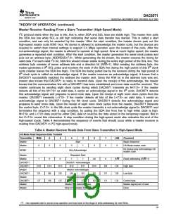
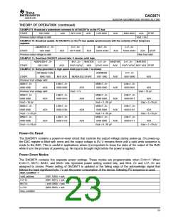
EXAMPLE 9: Broadcast a powerdown command to all DAC8571s on the I2C bus
START
1001 0000
ACK
0011 0101
ACK
1100 0000
ACK
0000 0000
ACK
STOP
Previous output voltage is valid
Vout = Hi-Z
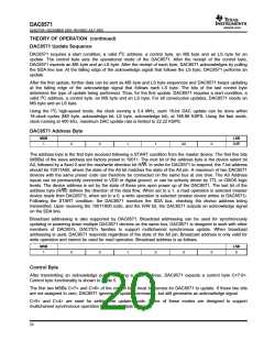
EXAMPLE 10: Broadcast update. All DAC8571s on the I2C bus update synchronously with the contents of their temporary
registers
ADDRESS <7...0>
1001 0000
C<7...0>
M<7...0>
L<7...0>
START
ACK
0011 0000
ACK
XXXX XXXX
ACK
XXXX XXXX
ACK
STOP
Previous output voltage is valid
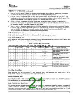
EXAMPLE 11: Read back DAC8571 internal data. V denotes valid logic.
New Vout valid
ADDRESS<7...0>
1001 1001
M<7...0>
MASTER
ACK
L<7...0>
MASTER
ACK
C<7...0>
MASTER
START
ACK
VVVV VVVV
VVVV VVVV
VVVV VVVV NOT ACK STOP
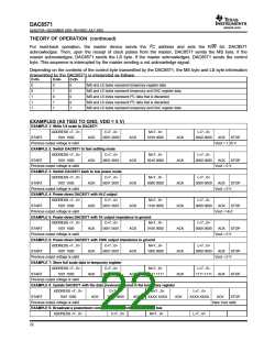
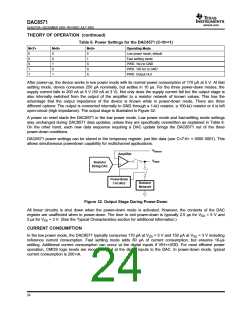
EXAMPLE 12: Ramp generation in high speed mode (up to code 7 is shown)
HS Master Code
0000 1000
ADDRESS
C<7...0>
START
NOT ACK
REPEATED START
1001 1000
ACK
ACK
ACK
0001 0000
ACK
Previous Vout voltage valid
MSB<7...0>
LSB<7...0>
0000 0000
MSB<7...0>
0000 0000
LSB<7...0>
0000 0001
0000 0000
ACK
ACK
ACK
Previous Vout voltage valid
MSB<7...0>
Vout = 0 V
Vout = 76 µV
LSB<7...0>
0000 0010
MSB<7...0>
0000 0000
LSB<7...0>
0000 0011
0000 0000
ACK
ACK
ACK
ACK
ACK
ACK
ACK
Vout = 76 µV
MSB<7...0>
0000 0000
Vout = 2 ×76 µV
MSB<7...0>
Vout = 3 ×76 µV
LSB<7...0>
0000 0100
LSB<7...0>
0000 0101
0000 0000
ACK
ACK
ACK
Vout = 3 ×76 µV
MSB<7...0>
0000 0000
Vout = 4 ×76 µV
MSB<7...0>
Vout = 5 ×76 µV
LSB<7...0>
0000 0110
LSB<7...0>
0000 0111
0000 0000
ACK
Vout = 5 ×76 µV
Vout = 6 ×76 µV
Vout = 7 ×76 µV
Power-On Reset
The DAC8571 contains a power-on-reset circuit that controls the output voltage during power-up. On power-up,
the DAC register is filled with zeros and the output voltage is 0V; it remains there until a valid write sequence is
made to the DAC. This is useful in applications where it is important to know the state of the output of the DAC
while it is in the process of powering up. No input is brought high before the power is applied.
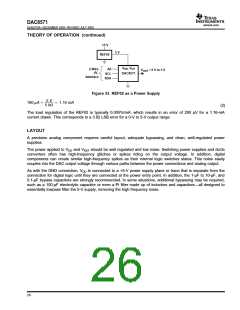
Power-Down Modes
The DAC8571 contains five separate power settings. These modes are programmable when C<0>=1. When
C<0>=1, M<7>, M<6>, and M<5> bits represent power setting control bits, and M<4...0> and L<7...0> are
assigned to zeroes. Power setting of DAC8571 is updated at the falling edge of the acknowledge signal that
follows the least significant byte. To set the power consumption of the device, following I2C sequence is used.
Start_condition ->
Valid_address
C<7:0>
(1001 1000) -> ack
(0001 0001) -> ack
( vvv0 0000) -> ack
(0000 0000) -> ack
M<7:0>
L<7:0>
Stop_condition
23

 TI [ TEXAS INSTRUMENTS ]