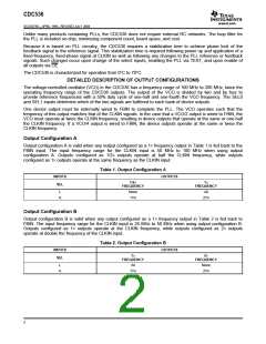
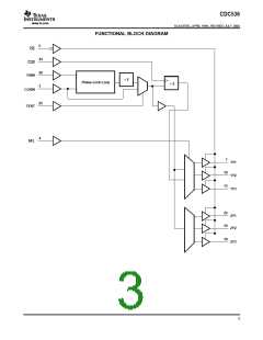
CDC536
www.ti.com
SCAS378G–APRIL 1994–REVISED JULY 2004
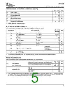
SWITCHING CHARACTERISTICS
over recommended ranges of supply voltage and operating free-air temperature, CL = 30 pF (see (1) and Figure 1 and
Figure 2)
FROM
(INPUT)
TO
(OUTPUT)
PARAMETER
MIN
MAX UNIT
fmax
Duty cycle
100
45%
500
MHz
55%
Y
Y
Y
(2)
tphase error
CLKIN↑
CLKIN↑
+500
200
0.5
1
ps
ps
ns
ns
ns
ns
Jitter(pk-pk)
(2)
tsk(o)
tsk(pr)
tr
tf
1.4
1.4
(1) The specifications for parameters in this table are applicable only after any appropriate stabilization time has elapsed.
(2) The propagation delay, tphase error, is dependent on the feedback path from any output to FBIN. The tphase error, tsk(o), and tsk(pk)
specifications are only valid for equal loading of all outputs.
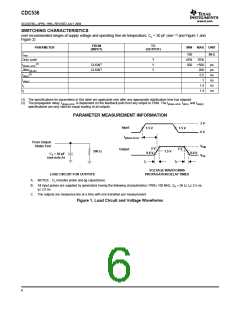
PARAMETER MEASUREMENT INFORMATION
3 V
0 V
Input
1.5 V
1.5 V
t
phase error
From Output
Under Test
V
V
OH
2 V
0.8 V
2 V
Output
500 W
1.5 V
0.8 V
C
= 30 pF
L
OL
(see note A)
t
r
t
f
VOLTAGE WAVEFORMS
PROPAGATION DELAY TIMES
LOAD CIRCUIT FOR OUTPUTS
A. NOTES: . CL includes probe and jig capacitance.
B. All input pulses are supplied by generators having the following characteristics: PRR≤ 100 MHz, ZO = 50 Ω, tr≤ 2.5 ns,
tf≤ 2.5 ns.
C. The outputs are measured one at a time with one transition per measurement.
Figure 1. Load Circuit and Voltage Waveforms
6

 TI [ TEXAS INSTRUMENTS ]