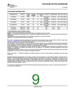
CDC536
www.ti.com
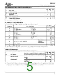
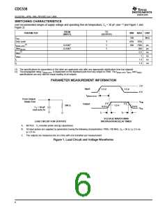
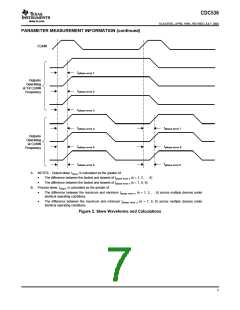
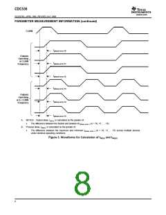
SCAS378G–APRIL 1994–REVISED JULY 2004
Unlike many products containing PLLs, the CDC536 does not require external RC networks. The loop filter for
the PLL is included on-chip, minimizing component count, board space, and cost.
Because it is based on PLL circuitry, the CDC536 requires a stabilization time to achieve phase lock of the
feedback signal to the reference signal. This stabilization time is required following power up and application of a
fixed-frequency, fixed-phase signal at CLKIN as well as following any changes to the PLL reference or feedback
signals. Such changes occur upon change of the select inputs, enabling the PLL via TEST, and upon enable of
all outputs via OE.
The CDC536 is characterized for operation from 0°C to 70°C.
DETAILED DESCRIPTION OF OUTPUT CONFIGURATIONS
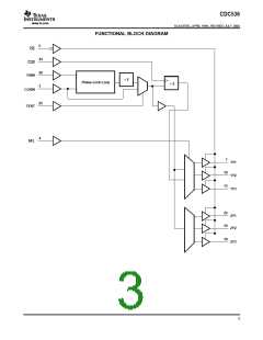
The voltage-controlled oscillator (VCO) in the CDC536 has a frequency range of 100 MHz to 200 MHz, twice the
operating frequency range of the CDC536 outputs. The output of the VCO is divided by two and by four to
provide reference frequencies with a 50% duty cycle of one-half and one-fourth the VCO frequency. The SEL0
and SEL1 inputs determine which of the two signals are buffered to each bank of device outputs.
One device output must be externally wired to FBIN to complete the PLL. The VCO operates such that the
frequency of this output matches that of the CLKIN signals. In the case that a VCO/2 output is wired to FBIN, the
VCO must operate at twice the CLKIN frequency, resulting in device outputs that operate at the same or one-half
the CLKIN frequency. If a VCO/4 output is wired to FBIN, the device outputs operate at the same or twice the
CLKIN frequency.
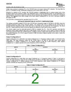
Output Configuration A
Output configuration A is valid when any output configured as a 1× frequency output in Table 1 is fed back to the
FBIN input. The input frequency range for the CLKIN input is 50 MHz to 100 MHz when using output
configuration A. Outputs configured as 1/2× outputs operate at half the CLKIN frequency, while outputs
configured as 1× outputs operate at the same frequency as the CLKIN input.
Table 1. Output Configuration A
INPUTS
SEL
OUTPUTS
1/2×
FREQUENCY
1×
FREQUENCY
L
None
1Yn
All
H
2Yn
Output Configuration B
Output configuration B is valid when any output configured as a 1× frequency output in Table 2 is fed back to
FBIN. The input frequency range for the CLKIN input is 25 MHz to 50 MHz when using output configuration B.
Outputs configured as 1× outputs operate at the CLKIN frequency, while outputs configured as 2× outputs
operate at double the frequency of the CLKIN input.
Table 2. Output Configuration B
INPUTS
SEL
OUTPUTS
1×
2×
FREQUENCY
FREQUENCY
L
All
None
2Yn
H
1Yn
2

 TI [ TEXAS INSTRUMENTS ]