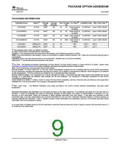
CDC536
www.ti.com
SCAS378G–APRIL 1994–REVISED JULY 2004
(1)
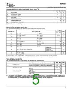
RECOMMENDED OPERATING CONDITIONS (SEE
)
MIN
3
MAX UNIT
VCC
VIH
VIL
VI
Supply voltage
3.6
V
V
High-level input voltage
Low-level input voltage
Input voltage
2
0.8
5.5
32
32
70
V
0
0
V
IOH
IOL
TA
High-level output current
Low-level output current
Operating free-air temperature
mA
mA
°C
(1) Unused inputs must be held high or low.
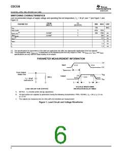
ELECTRICAL CHARACTERISTICS
over recommended operating free-air temperature range (unless otherwise noted)
TA = 25°C
PARAMETER
TEST CONDITIONS
II = -18 mA
UNIT
V
MIN MAX
VIK
VCC = 3 V,
1.2
VCC = MIN to MAX(1)
VCC = 3 V,
,
IOH = -100 µA
IOH = -32 mA
IOL = 100 µA
IOL = 32 mA
VI = 3.6 V
VCC-0.2
VOH
V
2
VCC = 3 V,
0.2
0.5
±10
±1
10
10
2
VOL
V
VCC = 3 V,
VCC = 0 or MAX(1)
,
II
µA
VCC = 3.6 V,
VI = VCC or GND
VO = 3 V
IOZH
IOZL
VCC = 3.6 V,
µA
µA
VCC = 3.6 V,
VO = 0
Outputs high
Outputs low
ICC
VCC = 3.6 V, IO = 0, VI = VCC or GND
2
mA
Outputs disabled
2
Ci
VI = VCC or GND
VO = VCC or GND
6
pF
pF
Co
9
(1) For conditions shown as MIN or MAX, use the appropriate value specified under recommended operating conditions.
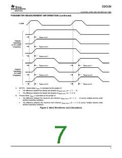
TIMING REQUIREMENTS
over recommended ranges of supply voltage and operating free-air temperature
MIN
MAX UNIT
When VCO is operating at four times the CLKIN frequency
When VCO is operating at double the CLKIN frequency
25
50
50
MHz
100
fclock
Clock frequency
Input clock duty cycle
40%
60%
50
After SEL
After OE↓
50
µs
50
Stabilization time(1)
After power up
After CLKIN
50
(1) Time required for the integrated PLL circuit to obtain phase lock of its feedback signal to its reference signal. In order for phase lock to
be obtained, a fixed-frequency, fixed-phase reference signal must be present at CLKIN. Until phase lock is obtained, the specifications
for propagation delay and skew parameters given in the switching characteristics table are not applicable.
5

 TI [ TEXAS INSTRUMENTS ]