CC2640R2L
ZHCSRK4A –APRIL 2020 –REVISED SEPTEMBER 2020
www.ti.com.cn
8 Specifications
8.1 Absolute Maximum Ratings
over operating free-air temperature range (unless otherwise noted)(1) (2)
MIN
MAX UNIT
VDDR supplied by internal DC/DC regulator or
internal GLDO. VDDS_DCDC connected to VDDS
on PCB
Supply voltage (VDDS, VDDS2,
and VDDS3)
4.1
V
V
–0.3
Supply voltage (VDDS(3) and
VDDR)
External regulator mode (VDDS and VDDR pins
connected on PCB)
2.25
–0.3
Voltage on any digital pin(4) (5)
VDDSx + 0.3, max 4.1
V
V
–0.3
–0.3
–0.3
–0.3
–0.3
Voltage on crystal oscillator pins, X32K_Q1, X32K_Q2, X24M_N and X24M_P
Voltage scaling enabled
VDDR + 0.3, max 2.25
VDDS
1.49
Voltage on ADC input (Vin)
Voltage scaling disabled, internal reference
Voltage scaling disabled, VDDS as reference
V
VDDS / 2.9
5
Input RF level
Tstg
dBm
°C
Storage temperature
150
–40
(1) All voltage values are with respect to ground, unless otherwise noted.
(2) Stresses beyond those listed under Absolute Maximum Ratings may cause permanent damage to the device. These are stress ratings
only, and functional operation of the device at these or any other conditions beyond those indicated under Recommended Operating
Conditions is not implied. Exposure to absolute-maximum-rated conditions for extended periods may affect device reliability.
(3) In external regulator mode, VDDS2 and VDDS3 must be at the same potential as VDDS.
(4) Including analog-capable DIO.
(5) Each pin is referenced to a specific VDDSx (VDDS, VDDS2 or VDDS3). For a pin-to-VDDS mapping table, see 表9-2.
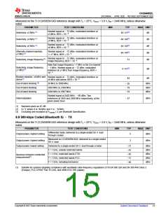
8.2 ESD Ratings
VALUE
UNIT
Human body model (HBM), per ANSI/ESDA/
JEDEC JS001(1)
All pins
±2500
Electrostatic discharge
VESD
V
(RHB and RGZ packages)
RF pins
±500
±500
Charged device model (CDM), per JESD22-
C101(2)
Non-RF pins
(1) JEDEC document JEP155 states that 500-V HBM allows safe manufacturing with a standard ESD control process.
(2) JEDEC document JEP157 states that 250-V CDM allows safe manufacturing with a standard ESD control process.
8.3 Recommended Operating Conditions
over operating free-air temperature range (unless otherwise noted)
MIN
MAX UNIT
Ambient temperature
85
°C
–40
Operating supply
voltage (VDDS and
VDDR), external
regulator mode
For operation in 1.8-V systems
(VDDS and VDDR pins connected on PCB, internal DC/DC cannot be used)
1.7
1.95
V
Operating supply
voltage VDDS
1.8
1.8
3.8
3.8
V
V
Operating supply
voltages VDDS2 and
VDDS3
For operation in battery-powered and 3.3-V systems
(internal DC/DC can be used to minimize power consumption)
VDDS < 2.7 V
Operating supply
voltages VDDS2 and
VDDS3
1.9
3.8
V
VDDS ≥2.7 V
Copyright © 2023 Texas Instruments Incorporated
Submit Document Feedback
11

 TI [ TEXAS INSTRUMENTS ]