CC1110Fx / CC1111Fx
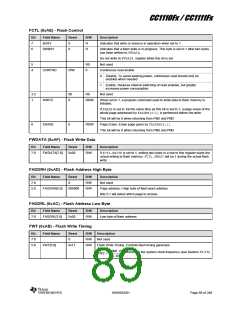
FCTL (0xAE) - Flash Control
Bit
7
Field Name
BUSY
Reset
R/W
R
Description
0
0
Indicates that write or erase is in operation when set to 1
6
SWBSY
R
Indicates that a flash write is in progress. This byte is set to 1 after two bytes
has been written to FWDATA.
Do not write to FWDATA register while this bit is set.
Not used
5
4
R0
0
CONTRD
R/W
Continuous read enable
0
Disable. To avoid wasting power, continuous read should only be
enabled when needed
1
Enable. Reduces internal switching of read enables, but greatly
increases power consumption.
3:2
1
00
0
R0
Not used
WRITE
ERASE
R0/W
When set to 1, a program command used to write data to flash memory is
initiated.
If ERASEis set to 1at the same time as this bit is set to 1, a page erase of the
whole page addressed by FADDRH[6:1]is performed before the write.
This bit will be 0 when returning from PM2 and PM3
Page Erase. Erase page given by FADDRH[5:1].
This bit will be 0 when returning from PM2 and PM3
0
0
R0/W
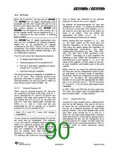
FWDATA (0xAF) - Flash Write Data
Bit
Field Name
Reset
R/W
Description
7:0
FWDATA[7:0]
0x00
R/W
If FCTL.WRITEis set to 1, writing two bytes in a row to this register starts the
actual writing to flash memory. FCTL.SWBSYwill be 1 during the actual flash
write
FADDRH (0xAD) - Flash Address High Byte
Bit
7:6
5:0
Field Name
Reset
0
R/W
R/W
R/W
Description
Not used
FADDRH[5:0]
000000
Page address / High byte of flash word address
Bits 5:1 will select which page to access.
FADDRL (0xAC) - Flash Address Low Byte
Bit
Field Name
Reset
R/W
Description
7:0
FADDRL[7:0]
0x00
R/W
Low byte of flash address
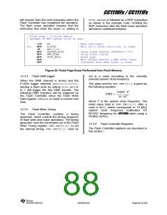
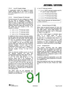
FWT (0xAB) - Flash Write Timing
Bit
7:6
5:0
Field Name
Reset
0
R/W
R/W
R/W
Description
Not used
FWT[5:0]
0x11
Flash Write Timing. Controls flash timing generator.
21000 F
16 109
, where F is the system clock frequency (see Section 12.3.5)
FWT
SWRS033H
Page 89 of 246

 TI [ TEXAS INSTRUMENTS ]