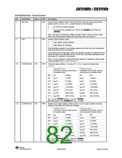
CC1110Fx / CC1111Fx
Setup DMA channel:
SRCADDR=<XDATA location>
DESTADDRR=FWDATA
VLEN=0
LEN=<block size>
WORDSIZE=byte
TMODE=single mode
TRIG=FLASH
SRCINC=yes
DESTINC=no
IRQMASK=yes
M8=0
PRIORITY=high
Setup flash address
Arm DMA Channel
Start flash write
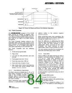
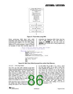
Figure 21: Flash Write using DMA
When performing DMA flash write while
executing code from within flash memory, the
instruction that triggers the first DMA trigger
event FLASH (TRIG[4:0]=10010) must be
aligned on a 2-byte boundary. Figure 22 shows
an example of code that correctly aligns the
instruction for triggering DMA (Note that this
code is IAR specific). The code below is
shown for CC1110Fx, but will also work for
CC1111Fx if the include file is being replaced by
ioCC1111.h
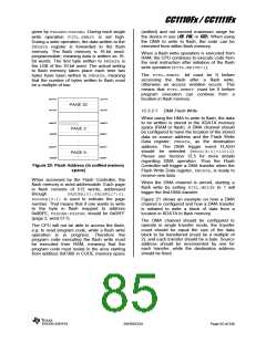
; Write flash and generate FLASH DMA trigger
; Code is executed from flash memory
;
#include “ioCC1110.h”
MODULE flashDmaTrigger.s51
RSEG RCODE (1)
PUBLIC halFlashDmaTrigger
FUNCTION halFlashDmaTrigger, 0203H
halFlashDmaTrigger:
ORL FCTL, #0x02;
RET;
END;
Figure 22: DMA Flash Write Executed from within Flash Memory
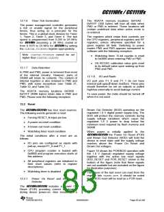
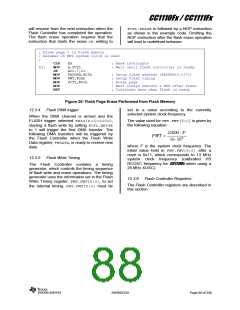
12.3.2.2 CPU Flash Write
to end within 40 μs after FCTL.SWBSY went
low and also within 40 μs after a write has
been initiated by writing a 1 to FCTL.WRITE
(see Figure 24). Failure to do so will clear the
FCTL.BUSY bit. FADDRH:FADDRL will contain
the address of the location where the write
operation failed. A new write operation can be
started by setting FCTL.WRITEto 1 again and
write two bytes to FWDATA. If one wants to do
the whole write operation over again and not
just start from where it failed, one has to erase
the page, writing the start address to
FADDRH:FADDRL, and setting FCTL.WRITE
to 1 (see Section 1.1.1).
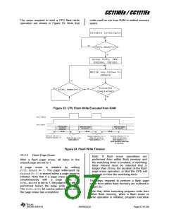
The CPU can also write directly to the flash
when executing program code from RAM using
unified memory space. The CPU writes data to
the Flash Write Data register, FWDATA. The
flash memory is written each time two bytes
have been written to FWDATA, if a write has
been enabled by setting FCTL.WRITE to 1.
The CPU can poll the FCTL.SWBSY status to
determine when the flash is ready for two new
bytes to be written to FWDATA.
Note that there exist a timeout period of 40 μs
for writing one flash word to FWDATA, thus
writing two bytes to the FWDATA register has
SWRS033H
Page 86 of 246

 TI [ TEXAS INSTRUMENTS ]