CC1110Fx / CC1111Fx
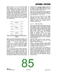
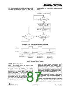
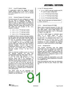
The steps required to start a CPU flash write
operation are shown in Figure 23. Note that
code must be run from RAM in unified memory
space.
Disable interrupts
YES
FCTL.BUSY=1?
NO
Setup FCTL, FWT,
FADDRH, FADDRL
Write two bytes to
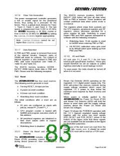
FWDATA
NO
YES
Transfer
Completed?
NO
FCTL.SWBSY=1?
YES
Figure 23: CPU Flash Write Executed from RAM
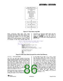
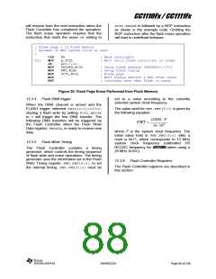
FCTL.SWBSY
FCTL.BUSY
Write two bytes
Write two bytes
to FWDATA
Write two bytes
to FWDATA
to FWDATA
(D0 and D1)
40 µs
40 µs
40 µs
Set FCTL.WRITE= 1
FADDRH:FADDRL= n
FADDRH:FADDRL= n + 1
Write D2 and D3 to
flash address n + 1
FADDRH:FADDRL= n + 2
Write D4 and D5 to
flash address n + 2
Write operation failed due
to a timeout.
Write D0 and D1 to
flash addres n
Figure 24. Flash Write Timeout
12.3.3
Flash Page Erase
Note: If flash erase operations are
performed from within flash memory and
the watchdog timer is enabled, a watchdog
timer interval must be selected that is
longer than 20 ms, the duration of the flash
page erase operation, so that the CPU will
manage to clear the watchdog timer.
After a flash page erase, all bytes in the
erased page are set to 1.
A
page erase is initiated by setting
FCTL.ERASE to 1. The page addressed by
FADDRH[5:1]is erased when a page erase is
initiated. Note that if a page erase is initiated
simultaneously with
a
page write, i.e.
The steps required to perform a flash page
erase from within flash memory are outlined in
Figure 25.
FCTL.WRITEis set to 1, the page erase will be
performed before the page write operation.
The FCTL.BUSYbit can be polled to see when
the page erase has completed.
Note that, while executing program code from
within flash memory, when a flash erase or
write operation is initiated, program execution
SWRS033H
Page 87 of 246

 TI [ TEXAS INSTRUMENTS ]