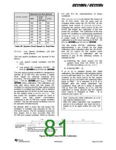
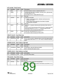
CC1110Fx / CC1111Fx
(unified) and not exceed maximum range for
the device in use (F8, F16, or F32). When using
the DMA to write to flash, the code can be
executed from within flash memory.
given by FADDRH:FADDRL. During each single
write operation FCTL.SWBSY is set high.
During a write operation, the data written to the
FWDATA register is forwarded to the flash
memory. The flash memory is 16-bit word-
programmable, meaning data is written as 16-
bit words. The first byte written to FWDATA is
the LSB of the 16-bit word. The actual writing
to flash memory takes place each time two
bytes have been written to FWDATA, meaning
that the number of bytes written to flash must
be a multiple of two.
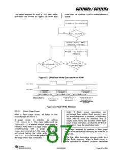
When a flash write operation is executed from
RAM, the CPU continues to execute code from
the next instruction after initiation of the flash
write operation (FCTL.WRITE=1).
The FCTL.SWBSY bit must be 0 before
accessing the flash after
a flash write,
otherwise an access violation occurs. This
means that FCTL.SWBSY must be 0 before
program execution can continue from
location in flash memory.
a
0x7FFE
0x7C00
0x7FFF
0x7C01
PAGE 32
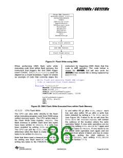
12.3.2.1 DMA Flash Write
.
.
.
When using the DMA to write to flash, the data
to be written is stored in the XDATA memory
space (RAM or flash). A DMA channel should
be configured to have the location of the stored
data as source address and the Flash Write
Data register, FWDATA, as the destination
address. The DMA trigger event FLASH
should be selected (TRIG[4:0]=10010).
Please see Section 12.5 for more details
regarding DMA operation. Thus the Flash
Controller will trigger a DMA transfer when the
Flash Write Data register, FWDATA, is ready to
receive new data.
0x0BFE
0x0800
0x0BFF
0x0801
.
.
.
.
.
.
PAGE 2
.
.
.
0x03FE
0x0000
0x03FF
0x0001
.
.
.
.
.
.
PAGE 0
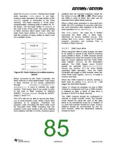
Figure 20: Flash Address (in unified memory
space)
When accessed by the Flash Controller, the
flash memory is word-addressable. Each page
in flash consists of 512 words, addressed
When the DMA channel is armed, starting a
flash write by setting FCTL.WRITE to 1 will
trigger the first DMA transfer.
through
FADDRH[0]:FADDRL[7:0].
FADDRH[5:1] is used to indicate the page
number. That means that if one wants to write
to the byte in flash mapped to address
0x0BFE, FADDRH:FADDRL should be 0x05FF
(page 2, word 511).
Figure 21 shows an example on how a DMA
channel is configured and how a DMA transfer
is initiated to write a block of data from a
location in XDATA to flash memory.
The DMA channel should be configured to
operate in single transfer mode, the transfer
count should be equal the size of the data
block to be transferred (must be a multiple of
2), and each transfer should be a byte. Source
address should be incremented by one for
each transfer, while the destination address
should be fixed.
The CPU will not be able to access the flash,
e.g. to read program code, while a flash write
operation is in progress. Therefore the
program code executing the flash write must
be executed from RAM, meaning that the
program code must reside in the area starting
from address 0xF000 in CODE memory space
SWRS033H
Page 85 of 246

 TI [ TEXAS INSTRUMENTS ]