CC1110Fx / CC1111Fx
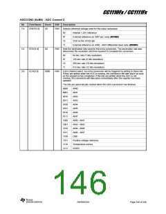
ADCCON3 (0xB6) - ADC Control 3
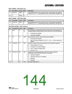
Bit
Field Name
Reset
R/W
Description
Selects reference voltage used for the extra conversion
7:6
EREF[1:0]
00
R/W
00
01
10
11
Internal 1.25V reference
External reference on AIN7 pin (only CC1110Fx)
VDD on the AVDD pin
External reference on AIN6 - AIN7 differential input (only CC1110Fx)
5:4
EDIV[1:0]
00
R/W
Sets the decimation rate used for the extra conversion. The decimation rate also
determines the resolution and time required to complete the conversion.
00
01
10
11
64 dec rate (7 bits resolution)
128 dec rate (9 bits resolution)
256 dec rate (10 bits resolution)
512 dec rate (12 bits resolution)
3:0
ECH[3:0]
0000
R/W
Extra channel select. An extra conversion will be triggered by writing to these bits.
If they are written while the ADC is running, the conversion will take place as soon
as the sequence has completed. If the bits are written while the ADC is not
running, the conversion will take place immediately after this register has been
updated.
The bits are automatically cleared when the extra conversion has finished.
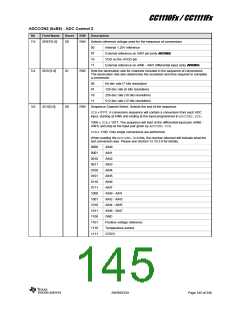
0000
0001
0010
0011
0100
0101
0110
0111
1000
1001
1010
1011
1100
1101
1110
1111
AIN0
AIN1
AIN2
AIN3
AIN4
AIN5
AIN6
AIN7
AIN0 - AIN1
AIN2 - AIN3
AIN4 - AIN5
AIN6 - AIN7
GND
Positive voltage reference
Temperature sensor
VDD/3
SWRS033H
Page 146 of 246

 TI [ TEXAS INSTRUMENTS ]