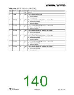
CC1110Fx / CC1111Fx
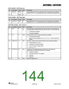
ADCL (0xBA) - ADC Data Low
Bit
Field Name
Reset
R/W
Description
7:4
ADC[3:0]
0000
R
Least significant part of ADC conversion result. The decimation rate configures
through ADCCON2.SDIVdetermines how many of these bits are relevant to use.
3:0
0000
R
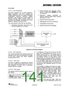
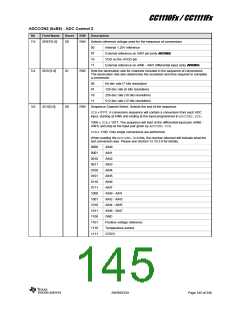
ADCH (0xBB) - ADC Data High
Bit
Field Name
Reset
R/W
Description
7:0
ADC[11:4]
0x00
R
Most significant part of ADC conversion result. The decimation rate configures
through ADCCON2.SDIVdetermines how many of these bits are relevant to use.
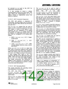
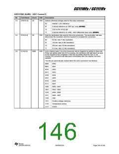
ADCCON1 (0xB4) - ADC Control 1
Bit
Field Name
Reset
R/W
Description
7
EOC
0
R
H0
End of conversion. Cleared when ADCH has been read. If a new conversion is
completed before the previous data has been read, the EOC bit will remain high.
0
1
Conversion not complete
Conversion completed
6
ST
0
R/W1
R/W
Start conversion. Read as 1 until conversion has completed
0
1
No conversion in progress
Start a conversion sequence if ADCCON1.STSEL=11and no sequence is
running.
5:4
STSEL[1:0]
11
Start select. Selects which event that will start a new conversion sequence.
00
01
10
11
External trigger on P2_0 pin.
Full speed. Do not wait for triggers.
Timer 1 channel 0 compare event
ADCCON1.ST=1
3:2
RCTRL[1:0]
00
R/W
Controls the 16 bit random generator. When set to 01, the setting will
automatically return to 00 when operation has completed.
00
01
10
11
Operation completed
Clock the LFSR once (13x unrolling)
Reserved
Reserved
1:0
11
R/W
Reserved. Always write 11
SWRS033H
Page 144 of 246

 TI [ TEXAS INSTRUMENTS ]