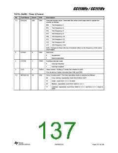
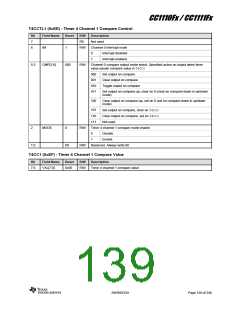
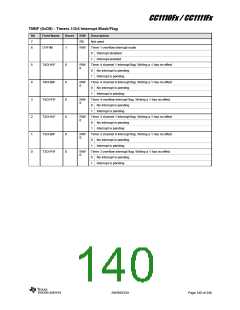
CC1110Fx / CC1111Fx
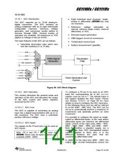
12.10 ADC
12.10.1 ADC Introduction
Eight individual input channels, single-
ended or differential (CC1111Fx has only
six channels)
The ADC supports up to 12-bit analog-to-
digital conversion. The ADC includes an
analog multiplexer with up to eight individually
configurable channels, reference voltage
generator, and conversion results written to
memory through DMA. Several modes of
operation are available. All references to VDD
applies to voltage on the pin AVDD.
Reference
voltage
selectable
as
internal, external single ended, external
differential, or VDD.
Interrupt request generation
DMA triggers at end of conversions
Temperature sensor input
The main features of the ADC are as follows:
Selectable decimation rates which also
sets the resolution (7 to 12 bits).
Battery measurement capability
AIN0
AIN7
Delta-Sigma
Modulator
Decimation
Filter
input
mux
VDD/3
TMP_SENSOR
Int 1.25V
AIN7
ref
mux
AVDD
Clock Generation and
Control
AIN6-AIN7
Figure 39: ADC Block Diagram
To configure a P0 pin to be used as an ADC
12.10.2 ADC Operation
input the corresponding bit in the ADCCFG
register must be set to 1. The default value in
this register disables the ADC inputs. Please
see Section 12.4.6.7 on Page 94 for more
details on how to configure the ADC input pins.
In the following these port pin will be referred
to as the AIN0 - AIN7 pins. The ADC can be
set up to automatically perform a sequence of
conversions and optionally perform an extra
conversion.
This section describes the general setup and
operation of the ADC and describes the usage
of the ADC control and status registers
accessed by the CPU.
12.10.2.1 ADC Core
The ADC is capable of converting an analog
input into a digital representation with up to 12
bits resolution. The ADC uses a selectable
positive reference voltage.
It is possible to configure the inputs as single-
ended or differential inputs. In the case where
differential inputs are selected, the differential
inputs consist of the input pairs AIN0 - AIN1,
AIN2 - AIN3, AIN4 - AIN5, and AIN6 - AIN7.
Note that neither a negative supply, nor a
supply larger than VDD (unregulated power)
can be applied to these pins. It is the
difference between the pairs that are
converted in differential mode.
12.10.2.2 ADC Inputs
The signals on the P0 port pins can be used as
ADC inputs.
Note: P0_6 and P0_7 do not exist on
CC1111Fx, hence only six input channels are
available (AIN0 - AIN5)
In addition to the input pins AIN0 - AIN7, the
output of an on-chip temperature sensor can
SWRS033H
Page 141 of 246

 TI [ TEXAS INSTRUMENTS ]