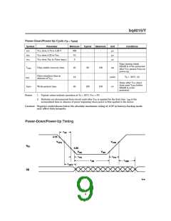
bq4015/Y
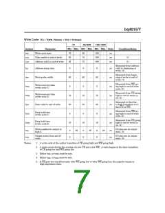
Write Cycle (T = T
, V
OPR CCmin
≤ V
CC
≤ V
)
CCmax
A
-70
-85/-85N
-120/-120N
Min. Max. Min. Max. Min. Max.
Symbol
tWC
Parameter
Write cycle time
Chip enable to end of write
Units
ns
Conditions/Notes
70
65
65
-
-
-
85
75
75
-
-
-
120
100
100
-
-
-
tCW
ns
(1)
(1)
tAW
Address valid to end of write
ns
Measured from address
valid to beginning of
write. (2)
tAS
Address setup time
0
55
5
-
-
-
-
-
-
-
0
65
5
-
-
-
-
-
-
-
0
85
5
-
-
-
-
-
-
-
ns
ns
ns
ns
ns
ns
ns
Measured from begin-
ning of write to end of
write. (1)
tWP
Write pulse width
Measured from WE go-
ing high to end of write
cycle. (3)
Write recovery time
(write cycle 1)
tWR1
tWR2
tDW
tDH1
Measured from CE going
high to end of write cy-
cle. (3)
Write recovery time
(write cycle 2)
15
30
0
15
35
0
15
45
0
Measured to first low-
to-high transition of ei-
ther CE or WE.
Data valid to end of write
Measured from WE go-
ing high to end of write
cycle. (4)
Data hold time
(write cycle 1)
Measured from CE going
high to end of write cy-
cle. (4)
Data hold time
(write cycle 2)
tDH2
10
10
10
Write enabled to output in
high Z
I/O pins are in output
state. (5)
tWZ
0
5
25
-
0
0
30
-
0
0
40
-
ns
ns
Output active from end of
write
I/O pins are in output
state. (5)
tOW
Notes:
1. A write ends at the earlier transition of CE going high and WE going high.
2. A write occurs during the overlap of a low CE and a low WE. A write begins at the later transition
of CE going low and WE going low.
3. Either tWR1 or tWR2 must be met.
4. Either tDH1 or tDH2 must be met.
5. If CE goes low simultaneously with WE going low or after WE going low, the outputs remain in
high-impedance state.
7

 TI [ TEXAS INSTRUMENTS ]