bq3285ED/LD
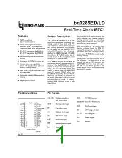
Block Diagram
X
X
1
Time-
Base
Oscillator
÷ 8
÷ 64
÷ 64
2
3
4
16 1 MUX
:
32K
INT
RST
32K
Driver
Control/Status
Registers
MOT
CS
Interupt
Generator
R/W
AS
Clock/Calendar, Alarm
and Control Bytes
µ
Bus
I/F
P
AD –AD
0
7
User Buffer
(14 Bytes)
DS
Control/Calendar
Update
Storage Registers
(114 Bytes)
RCL
Storage Registers
(128 Bytes)
EXTRAM
CS
V
V
Power-
Fail
Control
CC
OUT
BC
Write
Protect
BD328501.eps
AD0–AD7 Mu ltiplexed addr ess/data
in pu t/ou tpu t
Pin Descriptions
MOT
Bu s typ e select in p u t
The bq3285ED/LD bus cycle consists of two
phases: the address phase and the data-
transfer phase. The address phase pre-
cedes the data-transfer phase. During the
a d d r es s p h a s e, a n a d d r es s p la ced on
AD0–AD7 and EXTRAM is latched into the
bq3285ED/LD on the falling edge of the AS
signal. During the data-transfer phase of
the bus cycle, the AD0–AD7 pins serve as a
bidirectional data bus.
MOT selects bus timing for either Motorola
or Intel architecture. This pin should be
tied to VCC for Motorola timing or to VSS for
Intel timing (see Table 1). The setting
should not be changed during system opera-
tion. MOT is internally pulled low by a 30K
Ω resistor.
Table 1. Bus Setup
AS
Ad d r ess str obe in p u t
Bus
Type
MOT
DS
R/W
AS
AS serves to demultiplex the address/data
bus. The falling edge of AS latches the ad-
dress on AD0–AD7 and EXTRAM. This de-
multiplexing process is independent of the
CS signal. For DIP and SOIC packages
with MOT = VSS, the AS input is provided a
signal similar to ALE in an Intel-based sys-
tem.
Level Equivalent Equivalent Equivalent
DS, E, or
Motorola
VCC
R/W
AS
Φ2
RD,
WR,
Intel
VSS MEMR, or MEMW, or ALE
I/OR I/OW
July 1997
2

 TI [ TEXAS INSTRUMENTS ]