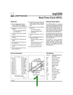
bq3285
DS
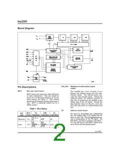
Data strobe input
RCL
RAM clear input
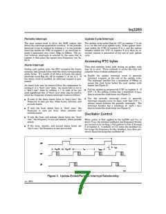
When MOT = VCC, DS controls data trans-
fer during a bq3285 bus cycle. During a
read cycle, the bq3285 drives the bus after
the rising edge on DS. During a write cycle,
the falling edge on DS is used to latch write
data into the chip.
A low level on the RCL pin causes the con-
tents of each of the 114 storage bytes to be
set to FF(hex). The contents of the clock
and control registers are unaffected. This
pin should be used as a user-interface input
(pushbutton to ground) and not connected
to the output of any active component. RCL
input is only recognized when held low for
at least 125ms in the presence of VCC when
the oscillator is running. Using RAM clear
does not affect the battery load. This pin is
connected internally to a 30KΩ pull-up re-
sistor.
When MOT = VSS, the DS input is provided
a signal similar to RD, MEMR, or I/OR in
an Intel-based system. The falling edge on
DS is used to enable the outputs during a
read cycle.
Read/write input
R/W
BC
3V backup cell input
When MOT = VCC, the level on R/W identi-
fies the direction of data transfer. A high
level on R/W indicates a read bus cycle,
whereas a low on this pin indicates a write
bus cycle.
BC should be connected to a 3V backup cell
for RTC operation and storage register non-
volatility in the absence of power. When
VCC slews down past VBC (3V typical), the
integral control circuitry switches the
power source to BC. When VCC returns
above VBC, the power source is switched to
When MOT = VSS, R/W is provided a signal
similar to WR, MEMW, or I/OW in an Intel-
based system. The rising edge on R/W
latches data into the bq3285.
VCC
.
Upon power-up, a voltage within the VBC
range must be present on the BC pin for
the oscillator to start up.
CS
Chip select input
CS should be driven low and held stable
during the data-transfer phase of a bus cy-
cle accessing the bq3285.
RST
Reset input
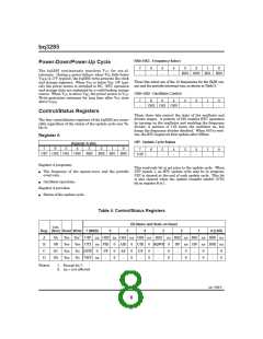
The bq3285 is reset when RST is pulled low.
When reset, INT becomes high-impedance,
and the bq3285 is not accessible. Table 4 in
the Control/Status Registers section lists
the register bits that are cleared by a reset.
INT
Interrupt request output
INT is an open-drain output. INT is as-
serted low when any event flag is set and
the corresponding event enable bit is also
set. INT becomes high-impedance whenever
register C is read (see the Control/Status
Registers section).
Reset may be disabled by connecting RST
to VCC. This allows the control bits to re-
tain their states through power-
down/power-up cycles.
SQW
Square-wave output
X1–X2
Crystal inputs
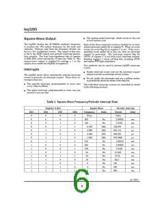
SQW may output a programmable fre-
quency square-wave signal during normal
(VCC valid) system operation. Any one of
the 13 specific frequencies may be selected
through register A. This pin is held low
when the square-wave enable bit (SQWE)
in register B is 0 (see the Control/Status
Registers section).
The X1–X2 inputs are provided for an ex-
ternal 32.768Khz quartz crystal, Daiwa
DT-26 or equivalent, with 6pF load capaci-
tance. A trimming capacitor may be neces-
sary for extremely precise time-base gen-
eration.
In the absence of a crystal, an oscillated
output of 32.768kHz can be fed into the X1
input.
Jan. 1999 E
3

 TI [ TEXAS INSTRUMENTS ]