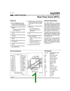
bq3285
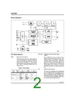
Block Diagram
AD0–AD7 Multiplexed address/data input/
output
Pin Descriptions
MOT
Bus type select input
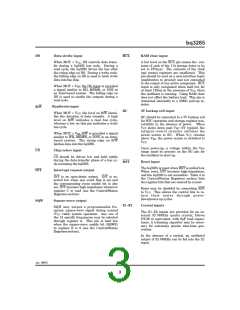
The bq3285 bus cycle consists of two
phases: the address phase and the data-
transfer phase. The address phase pre-
cedes the data-transfer phase. During the
address phase, an address placed on
AD0–AD7 is latched into the bq3285 on the
falling edge of the AS signal. During the
data-transfer phase of the bus cycle, the
AD0–AD7 pins serve as a bidirectional data
bus.
MOT selects bus timing for either Motorola
or Intel architecture. This pin should be
tied to VCC for Motorola timing or to VSS for
Intel timing (see Table 1). The setting
should not be changed during system opera-
tion. MOT is internally pulled low by a
30KΩ resistor.
Table 1. Bus Setup
AS
Address strobe input
Bus
Type
MOT
DS
R/W
AS
AS serves to demultiplex the address/data
bus. The falling edge of AS latches the ad-
dress on AD0–AD7. This demultiplexing pro-
cess is independent of the CS signal. For
DIP, SOIC, and PLCC packages with MOT =
VCC, the AS input is provided a signal simi-
lar to ALE in an Intel-based system.
Level Equivalent Equivalent Equivalent
DS, E, or
VCC
VSS
Motorola
R/W
WR,
AS
Φ2
RD,
Intel
MEMR, or MEMW, or ALE
I/OR
I/OW
Jan. 1999 E
2

 TI [ TEXAS INSTRUMENTS ]