bq25505
www.ti.com
SLUSBJ3B –AUGUST 2013–REVISED JANUARY 2014
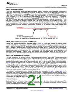
Push-Pull Multiplexor Drivers
There are two push-pull drivers intended to mulitplex between a primary non-rechargeable connected at
VBAT_PRI and secondary storage element connected on VBAT_SEC based on the VBAT_OK signal. When the
VBAT_OK signal goes high, indicating that the secondary rechargeable battery at VBAT_SEC is above the
VBAT_OK_HYST threshold, the VB_PRI_ON output goes high followed by the VB_SEC_ON signal going low in
order to connect VBAT_SEC to the system output (referred to as the VOR node). When VBAT_OK goes low,
indicating that the secondary rechargeable battery at VBAT_SEC is below the VBAT_OK threshold, the
VB_SEC_ON output goes high followed by the VB_PRI_ON signal going low in order to connect VBAT_PRI to
the system. The drivers are designed to support up to 2 nF of gate capacitance and to drive a PMOS FET. The
switching characteristics follow a break-before-make model, wherein during a transition, the drivers both go high
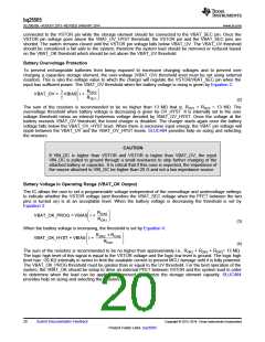
for a typical dead time of 5 us before one of the signals goes low. The figure below shows the FET gate voltages
for the transition from the secondary battery being connected to the system to the primary battery being
connected.
VB_PRI_ON
10ꢀsec
85%
85%
VB_SEC_ON
Figure 30. Break-Before-Make Operation of VB_PRI_ON and VB_SEC_ON
Steady State Operation and Cycle by Cycle Behavior
Steady state operation for the boost charger is shown in Figure 20. These plots highlight the inductor current
waveform, the VSTOR voltage ripple, and the LBOOST switching nodes. The charger uses hysteretic control and
pulse frequency modulation (PFM) switching in order to maintain high efficiency at light load. As long as the
VIN_DC voltage is above the MPPT regulation set point (i.e. voltage at VREF_SAMP), the boost charger's low-
side power FET turns on and draws current until it reaches its respective peak current limit. These switching
bursts continue until VSTOR reaches the VBAT_OV threshold. This cycle-by-cycle minor switching frequency is a
function of each converter's inductor value, peak current limit and voltage levels on each side of each
inductor. Once the VSTOR capacitor, CSTOR, droops below a minimum value, the hysteretic switching repeats.
Nano-Power Management and Efficiency
The high efficiency of the bq25505 charger is achieved via the proprietary Nano-Power management circuitry
and algorithm. This feature essentially samples and holds all references (except for VBAT_UV) in order to reduce
the average quiescent current. That is, the internal circuitry is only active for a short period of time and then off
for the remaining period of time at the lowest feasible duty cycle. A portion of this feature can be observed in
Figure 21 where the VRDIV node is monitored. Here the VRDIV node provides a connection to the VSTOR
voltage (first pulse) and then generates the reference levels for the VBAT_OV and VBAT_OK resistor dividers for
a short period of time. The divided down values at each pin are sampled and held for comparison against VBIAS
as part of the hysteretic control. Since this biases a resistor string, the current through these resistors is only
active when the Nano-Power management circuitry makes the connection—hence reducing the overall quiescent
current due to the resistors. This process repeats every 64 ms.
The bq25505's boost charger efficiency is shown for various input power levels in Figure 6 through Figure 12. All
data points were captured by averaging the overall input current. This must be done due to the periodic biasing
scheme implemented via the Nano-Power management circuitry. In order to properly measure the resulting input
current when calculating the output to input efficiency, the input current efficiency data was gathered using a
source meter set to average over at least 50 samples.
Thermal Shutdown
Rechargeable Li-ion batteries need protection from damage due to operation at elevated temperatures. The
application should provide this battery protection and ensure that the ambient temperature is never elevated
greater than the expected operational range of 85°C.
Copyright © 2013–2014, Texas Instruments Incorporated
Submit Documentation Feedback
21
Product Folder Links :bq25505

 TI [ TEXAS INSTRUMENTS ]