bq25505
www.ti.com
SLUSBJ3B –AUGUST 2013–REVISED JANUARY 2014
DETAILED DESCRIPTION
Boost Charger Overview
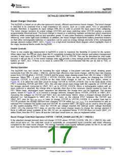
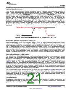
The bq25505 is based on an ultra low quiescent current, efficient synchronous boost charger. The boost charger
is intended to be powered from a high impedance DC source, such as a solar panel, TEG or piezoelectric
module; therefore, it regulates its input voltage (VIN_DC) in order to prevent the input source from collapsing.
The boost charger monitors its output voltage (VSTOR) and stops switching when VSTOR reaches a resistor
programmable threshold level. The boost charger is based on a switching regulator architecture which maximizes
efficiency while minimizing start-up and operation power. It uses pulse frequency modulation (PFM) to maintain
efficiency, even under light load conditions. In addition, the boost charger implements battery protection features
so that either rechargeable batteries or capacitors can be used as energy storage elements at the rechargeable
storage element output (VBAT_SEC). Figure 5 is a high-level functional block diagram which highlights most of
the major functional blocks inside the bq25505.
Enable Controls
There is one enable pin implemented in bq25505 in order to maximize the flexibility of control for the system.
When taken high, the EN pin shuts down the IC completely including the boost charger and battery management
circuitry. It also turns off the PFET that connects VBAT_SEC to VSTOR. This can be described as ship mode,
because it will put the IC in the lowest leakage state and provide a long storage period without discharging the
battery on VBAT_SEC. If there is no need to control EN, it is recommended that this pin be tied to VSS, or
system ground.
Startup Operation
The bq25505 has two circuits for boosting the input voltage, a low-power cold-start circuit, drawing power
exclusively from VIN_DC when ≥ VIN(CS), and the high efficiency main boost charger, with the bias rails drawing
power from VSTOR when ≥ VSTOR_CHGEN and the power stage drawing power from VIN_DC when ≥ VIN(DC)
minimum. When EN = 0 and VSTOR ≤ VSTOR_CHGEN, there are two options for charging the VSTOR
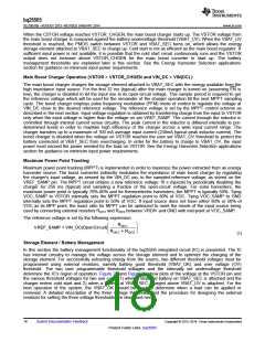
capacitor, CSTOR, to VSTOR_CHGEN for the main boost charger to turn on. The first option, shown in
Figure 28, is to allow the cold start circuit to charge VSTOR to VSTOR_CHGEN. Due to the body diode of the
PFET connecting VSTOR and VBAT_SEC, the cold start circuit must charge both the capacitor on CSTOR and
the storage element connected to VBAT_SEC up to VSTOR_CHGEN. When a rechargeable battery with an
open protector is attached, the charge time is typically short due to the minimum charge needed to close the
FET. When large, discharged super capacitors are attached, the charge time can be signficant. The second
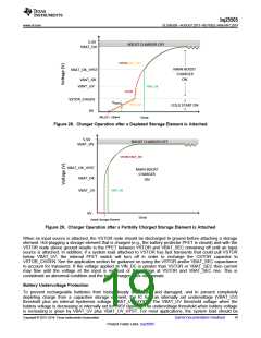
option, shown in Figure 29, is to connect a storage element, charged above VSTOR_CHGEN, to VBAT_SEC.
Assuming the voltages on VSTOR and VBAT_SEC are both below 100mV, when a charged storage element is
attached (i.e. hot-plugged) to VBAT_SEC, the IC turns on the internal PFET between the VSTOR and
VBAT_SEC pins for tBAT_HOT_PLUG in order to charge CSTOR to VSTOR_CHGEN. If a system load tied to
VSTOR prevents the storage element from charging VSTOR within tBAT_HOT_PLUG, it is recommended to add an
external PFET between the system load and VSTOR. An inverted VBAT_OK signal can be used to drive the gate
of this system-isolating PFET. Once the VSTOR pin voltage reaches the internal under voltage threshold
(VBAT_UV), the internal PFET stays on and the main boost charger begins to charge the storage element if
there is sufficient power available at the VIN_DC pin, as explained below. If VSTOR does not reach VBAT_UV
within 50ms, then the PFET turns off and the cold-start circuit turns on, also as explained below.
Boost Charger Cold-Start Operation (VSTOR < VSTOR_CHGEN and VIN_DC > VIN(CS) )
If the attached storage element does not charge CSTOR above VSTOR_CHGEN, VIN_DC ≥ VIN(CS), the cold-
start circuit turns on. The cold-start circuit is essentially an unregulated boost converter with lower efficiency
compared to the main boost charger. The energy harvester must supply sufficient power for the IC to exit cold
start. See the Energy Harvester Selection applications section for guidance.
Copyright © 2013–2014, Texas Instruments Incorporated
Submit Documentation Feedback
17
Product Folder Links :bq25505

 TI [ TEXAS INSTRUMENTS ]