bq24735
www.ti.com
SLUSAK9 –SEPTEMBER 2011
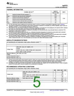
THERMAL INFORMATION
bq24735
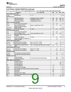
THERMAL METRIC(1)
UNITS
RGR (20 PIN)
(2)
θJA
Junction-to-ambient thermal resistance
46.8
56.9
46.6
0.6
θJCtop
θJB
Junction-to-case (top) thermal resistance(3)
Junction-to-board thermal resistance(4)
°C/W
ψJT
Junction-to-top characterization parameter(5)
(6)
ψJB
Junction-to-board characterization parameter
15.3
4.4
θJCbot
Junction-to-case (bottom) thermal resistance(7)
(1) For more information about traditional and new thermal metrics, see the IC Package Thermal Metrics application report, SPRA953.
(2) The junction-to-ambient thermal resistance under natural convection is obtained in a simulation on a JEDEC-standard, High-K board, as
specified in JESD51-7, in an environment described in JESD51-2a.
(3) The junction-to-case (top) thermal resistance is obtained by simulating a cold plate test on the package top. No specific JEDEC standard
test exists, but a close description can be found in the ANSI SEMI standard G30-88.
(4) The junction-to-board thermal resistance is obtained by simulating in an environment with a ring cold plate fixture to control the PCB
temperature, as described in JESD51-8.
(5) The junction-to-top characterization parameter, ψJT, estimates the junction temperature of a device in a real system and is extracted
from the simulation data for obtaining θJA, using a procedure described in JESD51-2a (sections 6 and 7).
(6) The junction-to-board characterization parameter, ψJB estimates the junction temperature of a device in a real system and is extracted
from the simulation data for obtaining θJA , using a procedure described in JESD51-2a (sections 6 and 7).
(7) The junction-to-case (bottom) thermal resistance is obtained by simulating a clod plate test on the exposed (power) pad. No specific
JEDEC standard test exists, but a close description can be found in the ANSI SEMI standard G30-88.
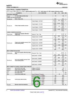
ABSOLUTE MAXIMUM RATINGS
over operating free-air temperature range (unless otherwise noted)(1)
(2)
VALUE
UNIT
MIN
–0.3
–2
MAX
30
SRN, SRP, ACN, ACP, CMSRC, VCC
PHASE
30
Voltage range
ACDET, SDA, SCL, LODRV, REGN, IOUT, ILIM, ACOK
BTST, HIDRV, ACDRV, BATDRV
–0.3
–0.3
–0.5
7
V
36
Maximum difference SRP–SRN, ACP–ACN
0.5
voltage
Junction temperature range, TJ
Storage temperature range, Tstg
–40
–55
155
155
°C
°C
(1) Stresses beyond those listed under absolute maximum ratings may cause permanent damage to the device. These are stress ratings
only, and functional operation of the device at these or any other conditions beyond those indicated under recommended operating
conditions is not implied. Exposure to absolute-maximum-rated conditions for extended periods may affect device reliability.
(2) All voltages are with respect to GND if not specified. Currents are positive into, negative out of the specified terminal. Consult Packaging
Section of the data book for thermal limitations and considerations of packages.
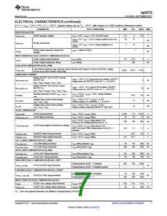
RECOMMENDED OPERATING CONDITIONS
over operating free-air temperature range (unless otherwise noted)
MIN
0
NOM MAX UNIT
SRN, SRP, ACN, ACP, CMSRC, VCC
PHASE
24
-2
24
V
Voltage range
ACDET, SDA, SCL, LODRV, REGN, IOUT, ILIM, ACOK
BTST, HIDRV, ACDRV, BATDRV
SRP–SRN, ACP–ACN
0
6.5
0
30
Maximum difference voltage
Junction temperature range, TJ
Storage temperature range, Tstg
–0.2
0
0.2
125
150
V
°C
°C
–55
Copyright © 2011, Texas Instruments Incorporated
Submit Documentation Feedback
5
Product Folder Link(s) :bq24735

 TI [ TEXAS INSTRUMENTS ]